
Introduction
This is part 2 of a 2-part series. The first part of this series requires the user to learn Multisim and create a firefly schematic. If you are not familiar with Multisim, please complete part 1 before attempting to use Ultiboard.
Published by Matt P. Lamparter with contributions from Ryder R. Nance.
-
-
Now that your circuit is complete in Multisim it is time to lay out the physical components on a printed circuit board.
-
We will begin by transferring all of the component and connection data from Multisim into Ultiboard via something called a netlist.
-
You will be given a custom PCB shape with several components already placed for you. You will be tasked with placing the remaining components and connecting them with traces on the PCB.
-
-
-
It is now time to familiarize yourself with Ultiboard. Begin by reading steps 5 and 6 in this NI tutorial: Introduction to Multisim/Ultiboard.
-
Note that we have already provided power and ground connectors for you so you may ignore this step in the tutorial.
-
-
-
Now download the partial PCB schematic file from the Maker-E Google drive.
-
Open the PCB file with Ultiboard.
-
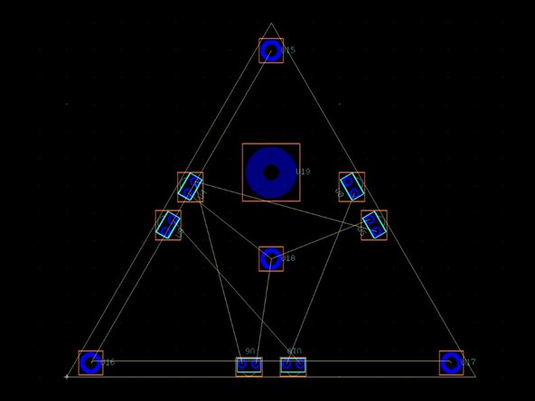
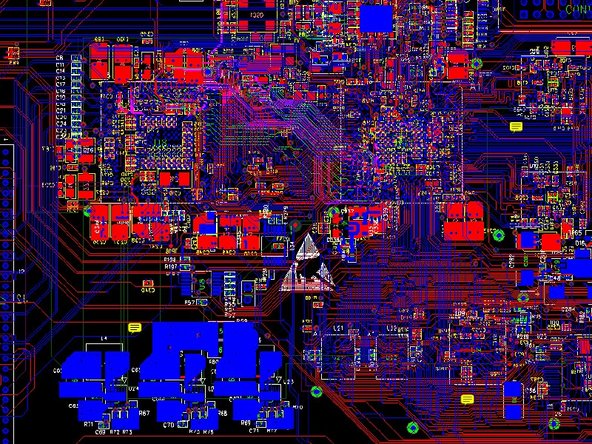
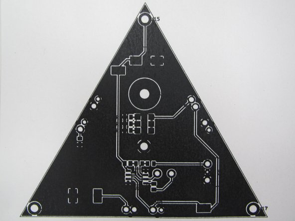
You are already given the PCB shape and several components in position: the IR emitters (LEDs)/detectors (phototransistor), the magnet, and the power supply pins.
-
Recall from the Multisim tutorial the discussion of refdes values. Note the refdes values shown in the example here: U4, U5, U6, U8, U9, U10, etc. These correspond to components in your Multisim file.
-
-
-
If you plan on using the PCB mill in the Maker-E to fabricate your board, you should follow the rules below to ensure the mill can successfully fabricate your PCB. Note that these issues are already taken care of in the firefly example.
-
Avoid “leadless” packages such as QFN if at all possible.
-
Make sure your traces are 0.4 mm or larger. It is possible to go as low as 0.2 mm with the mill, but traces this narrow have a high probability of failing during the milling process.
-
Try to choose packages with a pin pitch of 0.5 mm or larger. Packages with a pitch of 0.5 mm may require 0.2 mm traces.
-
If you will fabricate your board professionally (ie not in the Maker-E) your requirements are far less strict. But keep in mind that the smaller the component, the more difficult it will be to place on a PCB. Be sure to follow the design rules provided by the fabrication service you will use.
-
-
-
You are now ready to transfer your design from Multisim to Ultiboard. If you were creating a new PCB you would choose, from the Multisim menu bar, Transfer -> Transfer to Ultiboard -> Transfer to Ultiboard 14.0. This would create a default, rectangular PCB and you would need to resize the board to meet your specifications.
-
However, since we are providing you with a PCB file that already contains the correct dimensions, you will simply update this existing board with the changes you made in Multisim.
-
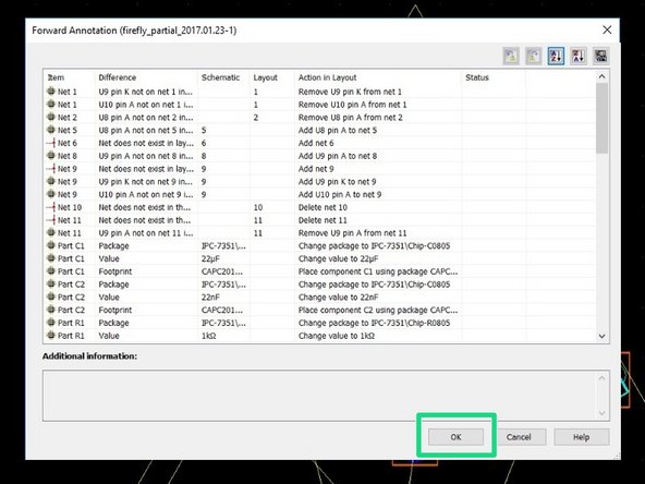
Perform this task by selecting Transfer -> Forward Annotate to Ultiboard -> Forward Annotate to Ultiboard 14.0.
-
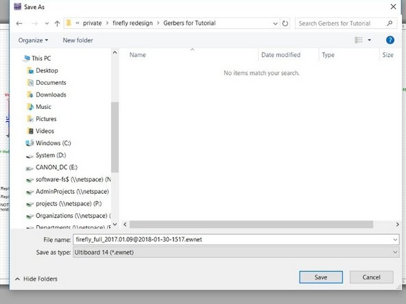
When prompted, save the netlist file wherever you have your Multisim and Ultiboard files saved.
-
Confirm component updates in Ultiboard by clicking OK when prompted.
-
-
-
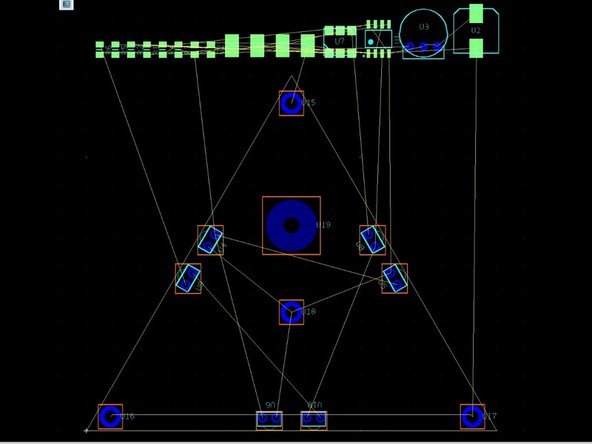
You now have all of the components you need to complete the firefly PCB. You will see the yellow “ratsnest” lines which indicate how components need to be connected. Your task now is to place all of the components within the bounds of the PCB and connect all of the components using traces on the top and bottom of the PCB.
-
When you are done, there should be no ratsnest remaining. Instead, all of these yellow virtual connections should be replaced with green and red traces.
-
If after forward annotating your Multisim file into the existing Ultiboard file you are missing any of the “orange boxed” components shown in this example, then there is an issue with your refdes values. Double check these values and make any changes necessary in order to make your Ultiboard PCB layout look like the example shown here.
-
The components surrounded by orange boxes have already been placed for you and are locked in place. These cannot be moved as they require precise placement in order to ensure proper circuit operation and communication with surrounding circuits.
-
-
-
There are a number of best practices you should keep in mind as you lay out your PCB. The following link will provide you with a summary of these best practices.
-
-
Note that the process used to realize plated through-holes in the Maker-E requires a slight modification to through-hole pads and drill holes. This will come into play when you begin through-hole traces on the top layer of your PCB. More on this later.
-
-
-
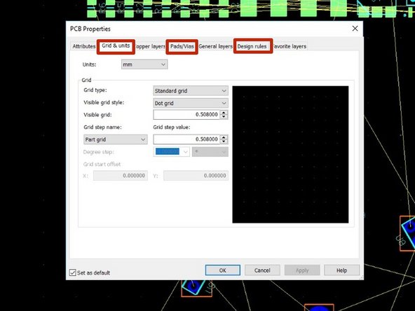
You should begin by setting your design rules in Ultiboard by opening Options -> PCB Properties.
-
Look at the Grid & Units, Pads/Vias, and Design rules tabs. These are the areas where you can configure the design rules and various settings and parameters for your PCB.
-
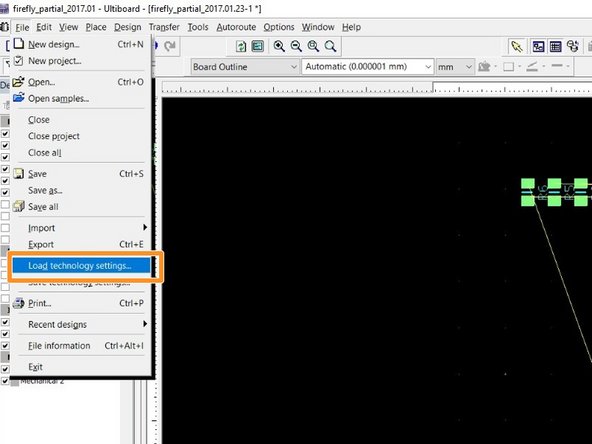
For the firefly PCB you can use this technology settings file which has most of these settings preconfigured. You will need to import this file into Ultiboard by choosing File -> Load technology settings.
-
-
-
Examine your schematic in Multisim and determine if it would make sense to use one or two power planes in your PCB.
-
Power planes minimize the number of traces needed by providing a large copper area where components can be directly connected to a specific net. Often power and ground are good uses for power planes, as many components require these connections. These planes can also provide protection from unwanted radio frequency interference.
-
You can use one plane per layer in your PCB. If you have a two layer PCB (what we use in the Maker-E) you can use up to two separate power planes (ie you can associate two different nets: one with the top layer and one with the bottom layer). You can also keep the same net associated with both layers, use only one plane, or none at all!
-
-
-
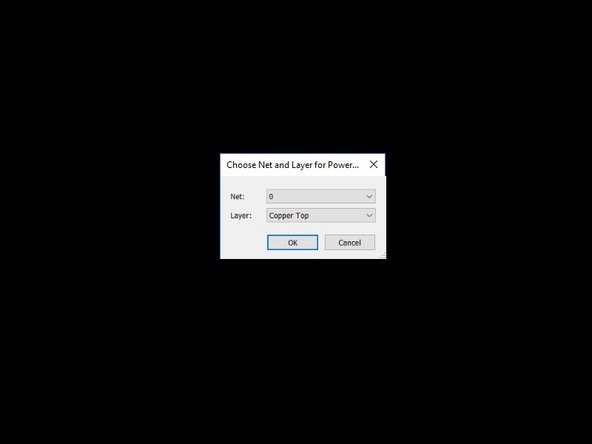
You can place a power plane by selecting Place -> Power plane from the menu bar. Ultiboard will then ask you to choose a net and layer for the plane.
-
The example shown here would make the entire top layer of the PCB into a ground plane. Hence, any time a pad on the top plane needed to be connected to ground it would simply connect to the top plane as opposed to creating a trace from this pad back to the common point where ground for the circuit was connected.
-
Note that adding a power plane to a copper layer does not mean that every connection and trace on that layer will connect to the power plane. Traces and pads that do not need connection to the power plane will remain isolated from the copper plane.
-
See the examples shown here in the second image. Note the black isolation around the pad labelled +. This pad is not connected to the ground plane while the other pads are connected to ground. The ground plane (right image) has rendered the previous trace (left image) redundant and thus it can be removed.
-
-
-
Adding a power plane may limit the amount of isolation you can have around traces and pads if you plan on milling your PCB in the Maker-E with the PCB mill. When you place a power plane in Ultiboard the default isolation width around everything is 0.254 mm.
-
This value corresponds to the width of the black isolation you see around all of the pads and traces in Ultiboard.
-
If you plan to mill your PCB in the Maker-E, and you are using a power plane, the mill will not allow you to cut isolation channels wider than this isolation value you define in Ultiboard.
-
If you intend to increase the isolation width during milling (recommended, as this will decrease the possibility of solder bridges) you will need to account for this isolation increase in Ultiboard first before moving to the mill.
-
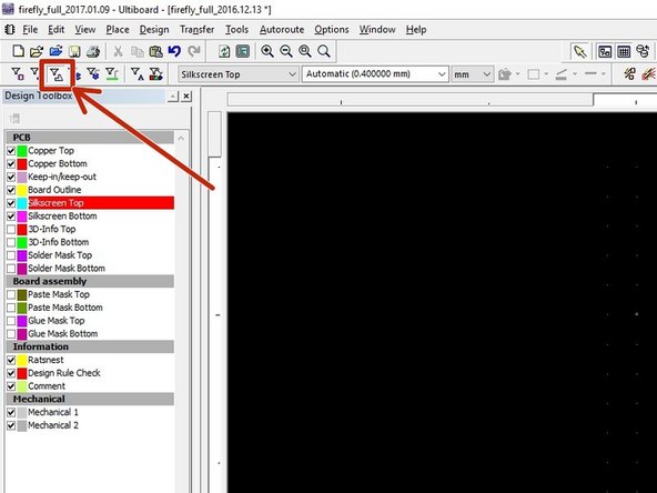
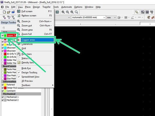
If you cannot see your power plane, you may not have copper areas enabled. Select View -> Copper areas. This menu can also be used to hide power planes from view if they are a distraction. This does not remove the planes from your design, just hides them for easier viewing.
-
-
-
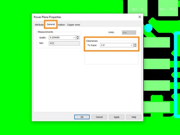
To change the isolation width, enable selecting copper areas and disable all other selection options.
-
In the Design Toolbox double click the layer where the power plane is placed to activate that layer. The layer text in the Design Toolbox should be highlighted in red to indicate it is the active layer. In this example we have activated the top layer.
-
Now right click on your PCB and choose Properties. Go to the General tab and change the To trace value from the default 0.254 mm to whatever value you desire for isolation around your pads.
-
Larger values translate to the possibility of more isolation when milling your PCB which can make soldering easier due to the decreased possibility of solder bridging to residual copper.
-
If you plan on using the 1 mm end mill bit in the Maker-E PCB mill (which is recommended in the PCB mill tutorial), you will need to change the To trace clearance value to at least 1 mm to provide the mill enough room to use the 1 mm end mill.
-
-
-
Use caution when increasing this clearance value. As you increase this value what you are in effect doing is removing more of your copper plane.
-
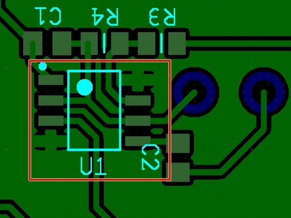
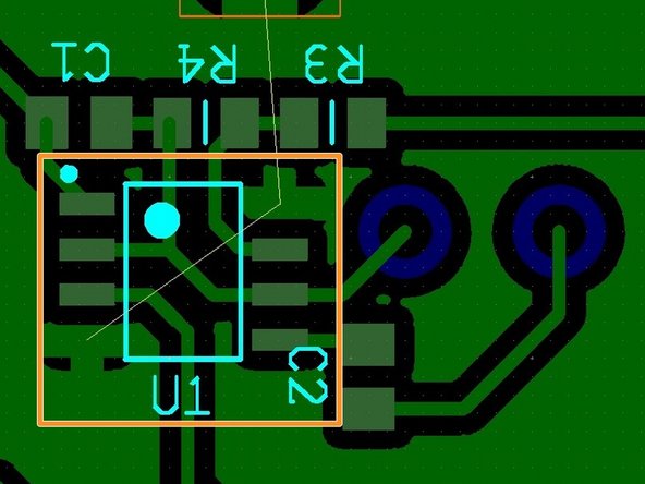
While this may make soldering easier, it can also cause connection issues by removing usable area for signals to flow on the plane. This comes into play when you inadvertently create “copper islands” or portions of the copper plane that are cut off from the rest of the plane by traces and large swathes of isolation.
-
See the example shown here for an illustration of this copper island effect.
-
Power plane with default clearance of 0.254 mm, no issues.
-
Power plane with clearance of 0.55 mm. Notice that pins 4 and 8 are now isolated from the main plane and thus require new traces for proper connection as evidenced by appearance of the yellow ratsnest. The pin 8 “island” is clearly visible while the pin 4 “island” is off screen.
-
Once you place power planes it can sometimes be difficult to see the other items on your PCB. If you wish to disable viewing the power planes (while still leaving the planes as part of the PCB) you can do so by choosing View -> Copper areas from the menu bar.
-
-
-
When you place your potentiometer (circular, adjustable resistor) and test points, be sure to position them so that they are easily accessible to fingers and scope probes. Keeping them close to the board edges is a good idea.
-
Now place your remaining components. Pay attention to the PCB Design Best Practices to make it as easy as possible to lay your traces.
-
-
-
You may wish to change the default trace width for certain nets, prior to laying traces. For example, perhaps you know that your power supply will be supplying high current to a particular device on your PCB. In this case you may want to increase the trace width for the power and ground nets to accommodate this high current.
-
Note that trace width is dependent upon the current it will carry and the thickness of the copper on the board. We use copper with a thickness of 1 oz/ft^2 in the Maker-E. You can find a PCB trace width calculator here. You will use the Results for External Layers in Air values. Pay attention to units.
-
-
-
If you wish to change the trace width for entire nets, click on the Nets tab at the bottom of the Ultiboard window. It may be convenient to drag the upper bound of this window vertically to enlarge the window.
-
Note that the units used for the net dimensions shown in the example here (0.4) are in millimeters. You can change the units for your board in the “Draw settings” toolbar.
-
As shown in this example, the default trace width for the firefly board is 0.4 mm which is sufficient for this circuit. If you wish to increase the width for a particular net, you can do so by double clicking the Trace width box in the corresponding net row and entering the desired value.
-
Note that you can select multiple nets by using the Shift and Ctrl keys. This allows you to change the width of multiples nets at once.
-
It is also possible to modify individual traces within a net by simply right clicking on them and changing the properties.
-
-
-
Once all of your components have been placed in such a way as to minimize ratsnest length and the number of ratsnest intersections, you are ready to begin laying traces.
-
Recall that every line in your ratsnest is a virtual connection: there is no physical connection yet, it is up to you to follow the ratsnest, determine where connections need to be made, and route traces from the beginning to the end of each ratsnest connection.
-
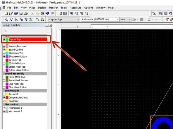
There are three methods of laying traces, ranging from completely manual to completely automatic. We will use the semi-automatic method. First, choose the layer where you wish to lay your trace (top or bottom) by double clicking it to make it active in the Design Toolbox.
-
-
-
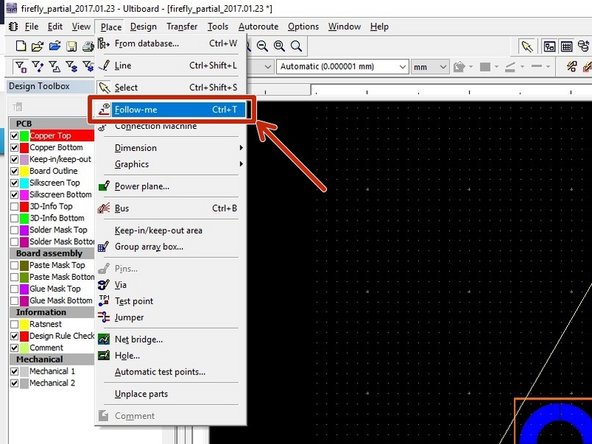
Now choose Place -> Follow-me from the toolbar. This method of placing traces will suggest possible automated routes, but allows you some flexibility in customizing these routes. It is a nice trade-off between automation and customization.
-
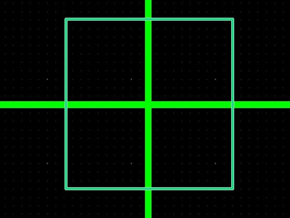
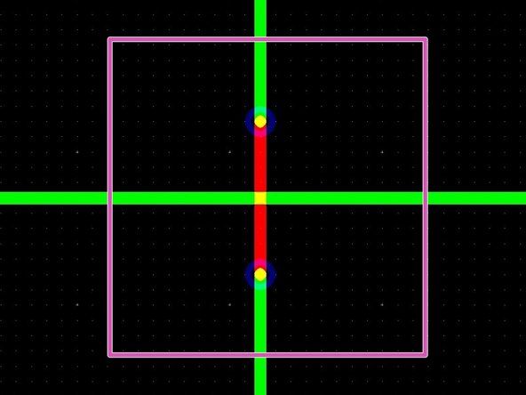
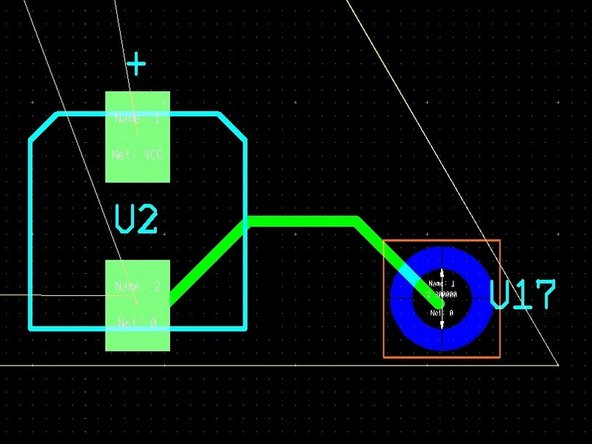
Follow-me will also prevent you from inadvertently making connections that are not part of your schematic. Remember that any time two traces come in contact on a single layer, you have made an electrical connection. So if you need to run traces perpendicular to each other without touching, you will first need to switch layers using a via:
-
The example highlighted in green shows overlapping traces on the same layer. These traces are connected.
-
The example highlighted in purple shows the use of vias to prevent traces from overlapping. The bottom layer is used in this case. These traces are not connected.
-
-
-
With Follow-me activated, single click where you would like your trace to begin. After you define a beginning point, Ultiboard will automatically suggest a possible route for your trace to follow to its destination. You can modify this suggested route by moving the cursor around the board.
-
If you wish to keep part of the suggested route and change another part, you can click on the PCB to anchor certain parts of the trace. When you click on the part of the PCB where the trace should end, the suggested route will become a defined route and your components will be connected.
-
-
-
Go through and connect the rest of your components until all of the ratsnest is gone. You will most likely need to use vias as you switch between top and bottom layers. Try to lay out your components in such a way as to minimize the number of vias you need.
-
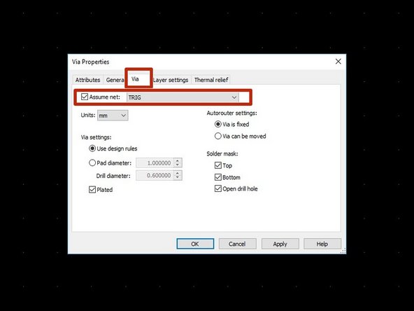
Note that after creating a via you should associate it with a net so that Follow-me will allow you to make connections to it.
-
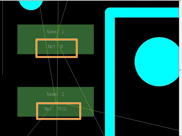
You can make net associations by right clicking on a via and choosing Properties. Within the Via tab, be sure to check the Assume net box and select the appropriate net.
-
You can view net names by zooming in on pads within Ultiboard to temporarily display a net name.
-
-
-
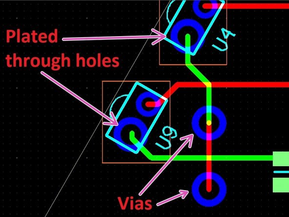
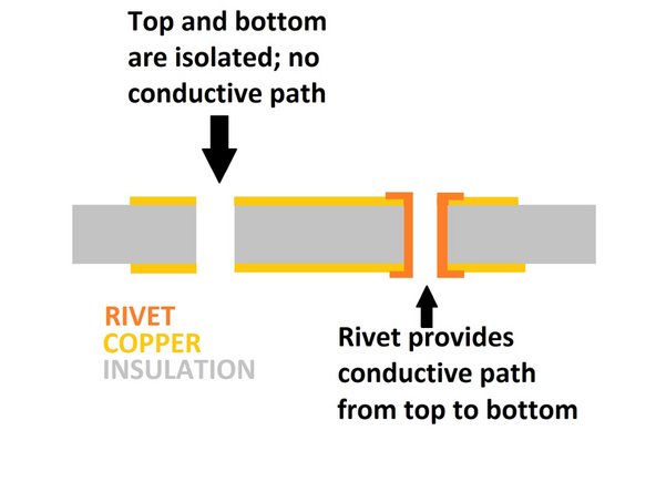
Vias and plated through holes (PTH) are common features of many PCBs. We have the ability to accomplish both of these in the Maker-E.
-
However, be aware that the method we use to realize both of these is different than that employed during professional PCB fabrication. Consequently, our design rules reflect this. The via design rules are listed in the PCB Design Best Practices document.
-
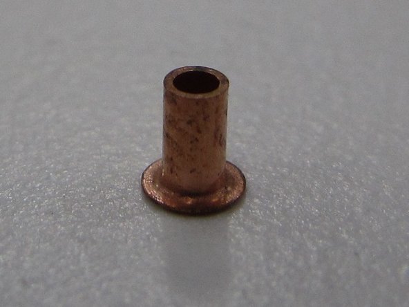
The method used to accomplish conductivity between copper layers is via small copper rivets, shown here in the second picture. These rivets require a hole of a particular size, plus an appropriately sized copper ring to accommodate the rivet flange. Failure to size vias/PTH properly will cause problems with your board.
-
Depending on how you design your board, many of the through hole components that you use will require vias (or plated through holes) in order to connect from the bottom to the top copper layer. Before continuing, PLEASE read this page. It will help you to determine where you need vias.
-
-
-
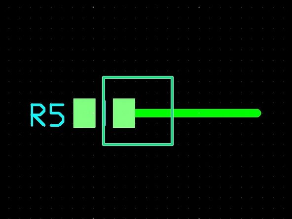
Keep in mind that traces for surface mount components should begin on the layer on which the component is mounted.
-
After beginning a trace on a SMT pad it is then possible to switch layers using a via.
-
A good example is shown highlighted in green. R5 is placed on the top layer, hence the pads are on the top layer, and the trace should begin on the top layer.
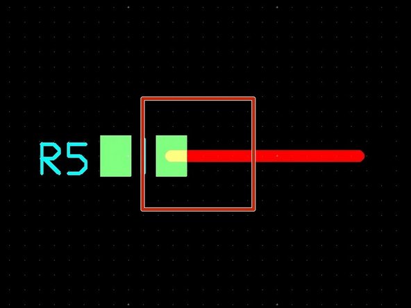
-
A bad example is shown highlighted in red. R5 is placed on the top layer, the pads are on the top layer, but the trace begins on the bottom layer. There is no connection!
-
If you inadvertently mix up layers, Ultiboard may place a via on top of a SMT pad for you in order to achieve connection. This is bad design practice for our process and should be avoided.
-
-
-
Traces for through hole components can begin on either side due to the nature of the plated through holes. However, boards fabricated in the Maker-E require extra attention to plated through holes.
-
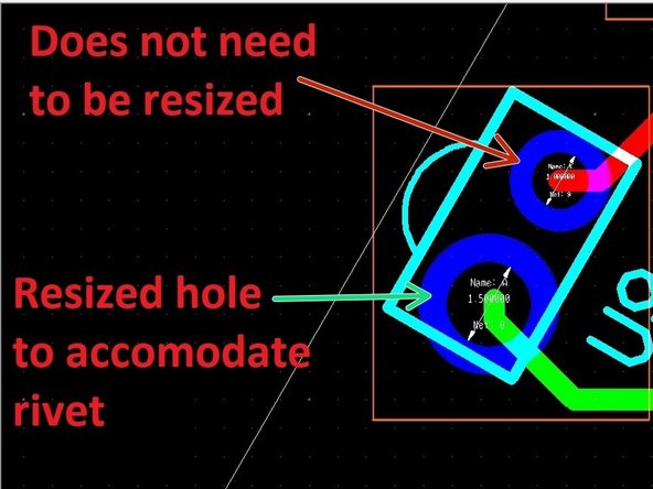
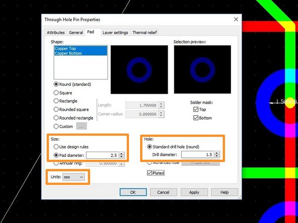
The process used in the Maker-E to realize through hole plating requires a hole size of 1.5 mm and a pad diameter of 2.5 mm.
-
If you have two adjacent pins with a standard spacing of 2.54 mm (0.1") you may reduce the pad diameter to 2.4 mm while maintaining a hole diameter of 1.5 mm. Ultiboard will generate a warning about this spacing, but you can ignore this warning. This is applicable to several components used in the firefly PCB.
-
Consequently, any time you wish to connect a trace to a through hole component lead on the top layer, you will need to modify the hole for this lead by right clicking on the hole, selecting Properties, and making the size changes in the Pad tab.
-
The reason behind this modification is due to the soldering process. Through hole components are soldered on the bottom of the board (when the component is placed on the top) so if a trace begins on the bottom there is electrical contact with the component lead when soldered on the bottom.
-
If a trace begins on the top layer, a board fabricated in the Maker-E will not initially provide conductivity from the bottom to the top because the hole is not plated with conductive material. The process required to achieve this conductivity necessitates enlarging the through hole size.
-
-
-
Take your time. Don’t be afraid to move components around or remove traces in favor of different routes as you begin to make connections on your PCB. Laying out a PCB is a bit of an art and you will become better with practice.
-
Again, refer to the PCB Design Best Practices for additional tips for beginners located at the bottom of the document.
-
-
-
When you have all of your components placed, all of your traces run, and all of the ratsnest has been eliminated then you have completed your PCB design. Take a break, get some coffee, and then double check your design.
-
-
-
Before proceeding on to manufacture your board it is crucial to print out your entire PCB on paper, place all of your components on the PCB, and make sure that all of your footprints are correct.
-
A significant amount of money and time can be saved when these errors are caught on paper as opposed to a PCB. If you find that a part does not fit on top of a footprint the way you anticipated, you need to:
-
go back to Multisim and choose the correct package, then forward annotate to update Ultiboard or
-
adjust the footprint you created to correct the errors.
-
-
-
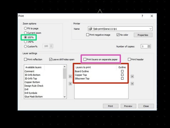
To print your PCB, select File -> Print from the menu bar.
-
Be sure to follow these steps in the order shown below:
-
Select the layers you want to appear on the printed page by moving them from the left box to the right box. You should print these layers: board outline, silkscreen top, copper top
-
Select a zoom level of 100%
-
Uncheck the Print layers on separate paper box
-
If you do not move layers into the right box first, you will not be able to change the zoom options.
-
-
-
If your PCB contains power planes, these planes will print out as solid black areas as part of the “copper top” layer. This is intentional.
-
However, if you find this distracting you can temporarily delete your power planes by:
-
disabling all selection tools and enabling only the Select copper areas tool ,
-
activating the layer you wish to remove by double clicking its layer name in the Design Toolbox,
-
enabling View -> Copper areas,
-
clicking on the copper area of your PCB to select it and then pressing Delete.
-
Deleting your power planes will cause several components to lose connection to the associated net and thus many ratsnest connections will appear. You can ignore these. Just be sure to add the plane(s) back when you are done printing!
-
-
-
Once you are sure that your PCB is correct, that all of your footprints are the right size and you have all of your traces properly run, it is time to export the PCB for fabrication.
-
Regardless of where your PCB will be fabricated, the process is the same. The industry standard file type for PCB fabrication of the board layers is the Gerber file. There is a separate file used for drilling the holes in your PCB called an NC drill file which is typically in the Excellon format.
-
Each layer in your PCB will export to a separate Gerber file. One file for the top copper layer, one file for the bottom copper layer, one file for the board outline, etc. There will also be a separate NC drill file.
-
-
-
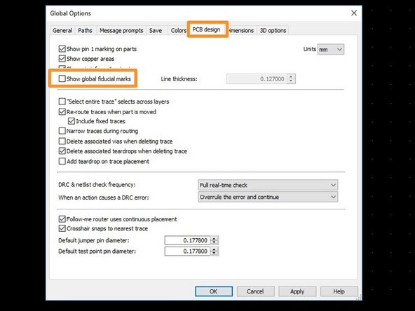
Prior to exporting Gerber files, it is necessary to turn off special markers known as Fiducial Markers. These markers will be discussed in more detail in the PCB Milling tutorial. For now we need to disable them.
-
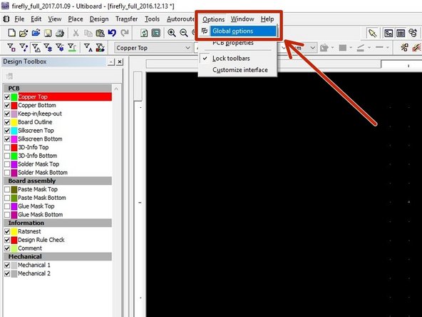
Open the PCB Design options window by clicking on Options -> Global options within the menu bar.
-
Navigate to the PCB Design tab and uncheck the box next to Show global fiducial marks.
-
Click OK when you are finished.
-
-
-
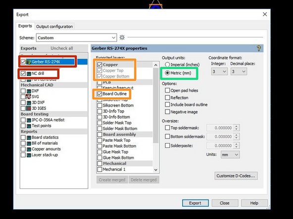
To export your Gerber files, select File -> Export from the menu bar. In the left box of the window that appears, be sure to check the boxes for Gerber RS-274X and NC drill.
-
Pay attention to the following items in the properties portion of the export window:
-
Check the box for Copper top
-
Check the box for Copper bottom
-
Check the box for Board Outline
-
All other layers should be unchecked.
-
Check the box for Metric output units if you will be using the PCB mill in the Maker-E. Otherwise, consult the recommendations of the board house you are using.
-
If your PCB will be professionally manufactured you will also want to export solder mask and silkscreen layers.
-
-
-
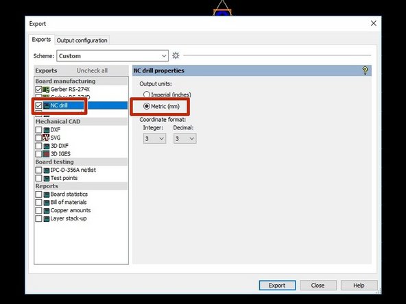
After configuring the options for the Gerber files, click on the NC drill option in the Exports box and make sure that the output units match those chosen for the Gerber files. For the PCB mill in the Maker-E this will be Metric.
-
-
-
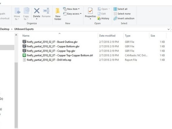
After configuring all of the options, click Export.
-
By default your Gerber files will be exported to a newly created folder called Ultiboard Exports as a subdirectory within the folder where your Ultiboard project file is saved. Navigate to this folder and confirm that you have the following five files:
-
yourProjectName - Board Outline.gbr
-
yourProjectName - Copper Bottom.gbr
-
yourProjectName - Copper Top.gbr
-
yourProjectName - Copper Top-Copper Bottom.drl
-
yourProjectName - Drill Info.rep
-
-
-
Congratulations! You just designed your first PCB. If you feel your design is complete, please contact the Lab Director for review before proceeding on to the PCB mill tutorial.
-
Be sure to email your Ulitboard project file (*.ewprj) to the Lab Director for review.
-


Cancel: I did not complete this guide.
9 other people completed this guide.
Team
2 Comments
Do you have the same coordinate format between both? For example 3:3 or 3:4?
Matt P. Lamparter - Resolved on Release Reply