
Introduction
The definition of and theory behind PCB design and layout is beyond the scope of this document. Throughout the tutorial there are links for additional reading. The user is encouraged to explore these resources to gain additional insight into the practice of PCB design. If you are interested in the process used to fabricate professional PCBs, please visit this link from Advanced Circuits.
Published by Matt P. Lamparter with contributions from Ryder R. Nance and Alan Cheville.
-
-
All methods of PCB fabrication will have limitations and tolerances associated with the processes used. These are typically accounted for in a set of Design Rules.
-
Below are some guidelines when designing PCBs that will ultimately be milled using the ProtoMat S103 in the Maker-E:
-
Try to keep traces at 0.4 mm or wider. The mill can handle traces down to 0.2 mm in width, but the reliability of these traces decreases at this narrow width.
-
When choosing SMT components, try to select packages that have a pin pitch of 0.5 mm or larger. Pitches below 0.5 mm may result in pads that are too narrow or are completely removed by the milling tools.
-
Use the following drill hole sizes (in mm): 0.6, 0.9, 1.0, 1.2, 1.4, 1.5, 1.6, 2.0, 3.0. Tools for holes outside of these sizes may be available, but will require the assistance of the Lab Director or a Maker-E tech.
-
-
-
Single or double sided PCBs are possible using the ProtoMat S103.
-
The board material used in the Maker-E is composed of two layers of copper (1 oz. weight - 36 μm copper thickness) separated by an insulating layer of FR4. The entire board thickness is 1.6 mm (or 1/16”).
-
Connections between top and bottom layers are achieved through connecting holes called vias. Note that this connection is not automatic and additional steps are required to achieve this connection. More on this later.
-
-
-
The mill uses a subtractive process to remove small amounts of copper from a sheet of copper clad board.
-
By removing copper from specific areas, electrical isolation can be achieved and discrete connections can be made between components.
-
The mill can create PCBs that incorporate both through hole and surface mount components.
-
-
-
The CircuitPro software used to define toolpaths and operate the mill is available on all ECE lab computers, including those found in Dana 303, 305, 307 and BRKI 163, as well as the rest of the Maker-E.
-
A large portion of the time required in using the mill is consumed with using CircuitPro to define toolpaths. In order to avoid long wait times when using the mill, it is required that you perform the following toolpath generation steps on a computer in one of the previously suggested locations.
-
Do not use the mill computer to generate toolpaths. This will create a bottleneck and prevent other makers from using the PCB mill.
-
After completing toolpath generation elsewhere, you may bring your completed CircuitPro file to the PCB mill computer.
-
The mill computer is not connected to the internet. Please bring your CircuitPro file on a flash drive. There is one provided at the mill if you need one. You cannot use network services such as Google Drive or Netspace.
-
-
-
Begin by logging in to a computer in the Maker-E or an ECE lab. Launch the CircuitPro application.
-
-
-
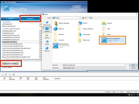
We will use a custom template tailored specifically for our process in the Maker-E. This template file is available on the Google Drive. Please download the file here.
-
Once you have the template file, navigate to the Templates tab in CircuitPro and click the Load custom template button.
-
Select the Maker-E_Template.cbf file you downloaded from the Maker-E Google drive.
-
-
-
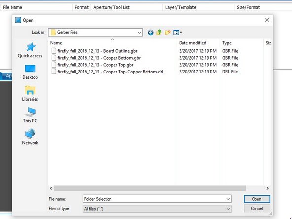
The first step is to import the Gerber files associated with the PCB you wish to mill. Please see the PCB Design Tutorial for exporting Gerber files from Ultiboard.
-
Click the Import button to import your Gerber files.
-
Any EDA software can be used to create your PCB, such as Eagle or Altium Designer. However, as the Maker-E only officially supports Ultiboard, you will need to determine on your own how to export Gerber files from your EDA if you use something other than Ultiboard.
-
If you do not have a set of your own Gerber files, and you do not wish to complete the PCB Design Tutorial, you may download a set of Gerber files from the Maker-E Google Drive.
-
-
-
You will need four files (layers):
-
Board outline
-
Copper bottom
-
Copper top
-
NC drill file (*.drl)
-
Highlight your files (use Ctrl or Shift on the keyboard to choose multiple files) and click Open.
-
-
-
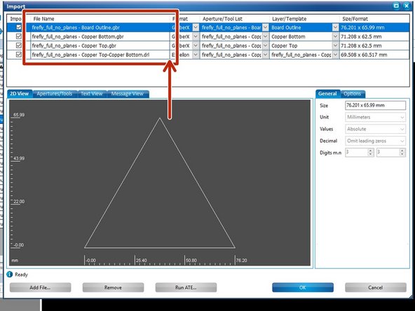
Now you need to map each Gerber file to a board layer within CircuitPro. The official names for these layers in CircuitPro are (note that there are no spaces between words):
-
BoardOutline
-
TopLayer
-
BottomLayer
-
DrillUnplated
-
You should drag the File name column to the right so that you can view the full file name of your Gerber files. If you exported your Gerber files from Ultiboard then the file names include the layer names appended at the end of the file name.
-
It is imperative that you map the correct files to the proper layers in CircuitPro. This is why it is important to be able to read the full file name when mapping.
-
-
-
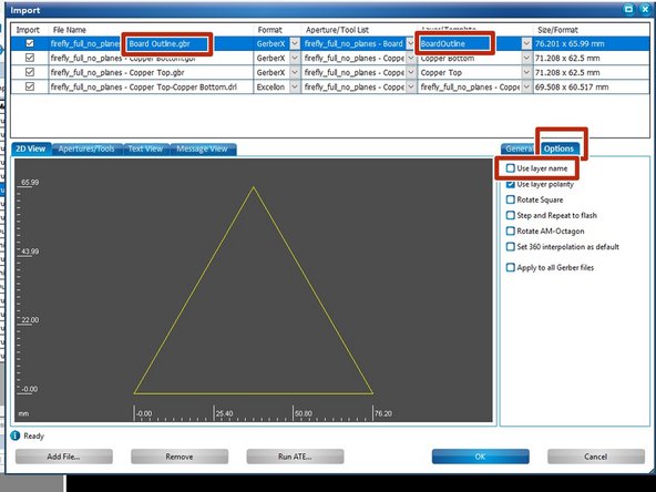
Begin with the first file, your board outline, which should end in "- Board Outline.gbr" if you exported from Ultiboard. Within the Options tab, deselect Use layer name.
-
Next, pull down the Layer/Template menu for your board outline file and choose the BoardOutline layer. The image of the outline should turn yellow.
-
You have just assigned your board outline Gerber file to the “BoardOutline” layer in CircuitPro.
-
-
-
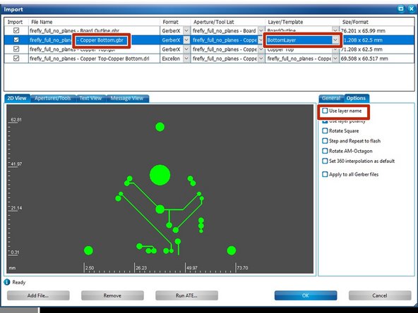
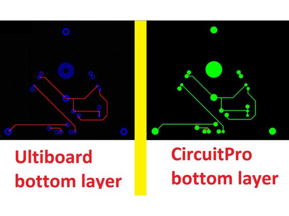
Now move on to your copper bottom file, which should end in "- Copper Bottom.gbr" if you exported from Ultiboard. Within the Options tab deselect Use layer name.
-
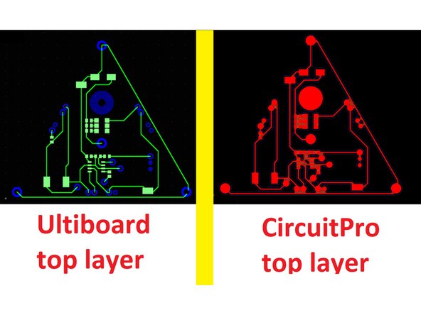
Next, pull down the Layer/Template menu for your copper bottom file and choose the BottomLayer layer. The image of the bottom copper layer should turn green. Note that this layer was red in Ultiboard.
-
You have just assigned your copper bottom Gerber file to the “BottomLayer” layer in CircuitPro.
-
If your PCB contains a power plane on the bottom layer you may see a nearly entirely green image. This green area corresponds to the copper in your power plane.
-
-
-
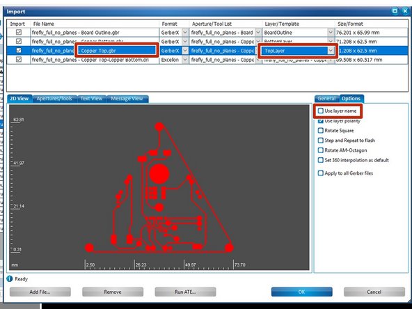
Now move on to your copper top file, which should end in "- Copper Top.gbr" if you exported from Ultiboard. Within the Options tab deselect Use layer name.
-
Next, pull down the Layer/Template menu for your copper top file and choose the TopLayer layer. The image of the top copper layer should turn red. Note that this layer was green in Ultiboard.
-
You have just assigned your copper top Gerber file to the “TopLayer” layer in CircuitPro.
-
If your PCB contains a power plane on the top layer you may see a nearly entirely red image. This red area corresponds to the copper in your power plane.
-
-
-
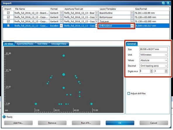
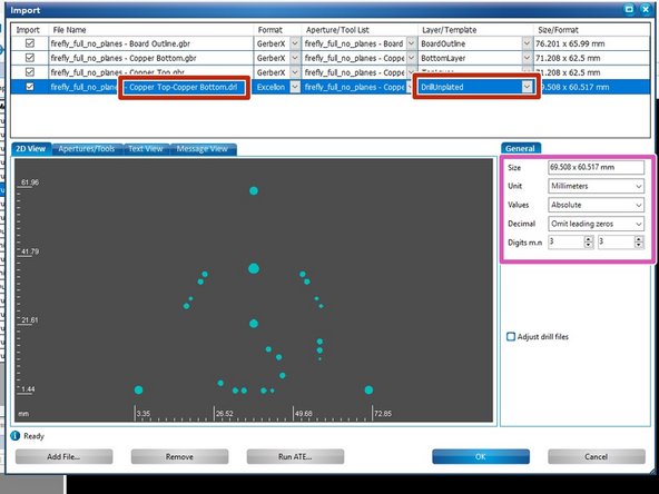
Finally, move on to your NC drill file, which should end in "- Copper Top-Copper Bottom.drl" if you exported from Ultiboard. Pull down the Layer/Template menu for your drill file and choose the DrillUnplated layer. The image of the drill holes should turn teal.
-
You have just assigned your NC drill file to the “DrillUnplated” layer in CircuitPro. If the pattern of drill holes does not match what you expect, check the settings under the General tab and make sure they match the settings shown here in the example.
-
Click OK to finish importing your files.
-
-
-
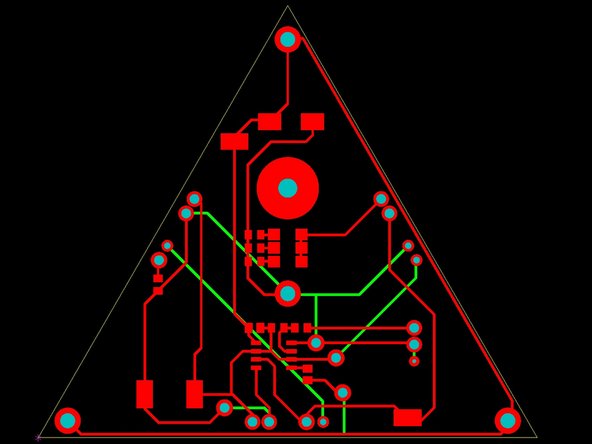
You should now see your PCB on the screen, complete with all of the layers. Note that the colors red and green will be inverted from what they were in Ultiboard (the top copper layer is now red and the bottom copper layer is green).
-
Make sure that all of the layers and holes line up properly. If anything is misaligned your board will not mill properly. The most likely cause for misalignment is a difference in the units (metric vs imperial) used in your Gerber and NC drill files.
-
-
-
If everything on your PCB looks OK (layers and holes are aligned, etc.), the next step is to add fiducials. In the milling process, fiducials are used to properly align the copper clad material when it is flipped over during milling and drilling of opposite sides.
-
The mill uses a camera that looks for these marks and makes any adjustments necessary when changing board sides in order to account for board rotation and translation. Without this alignment process it would be nearly impossible to have the two sides of your PCB align!
-
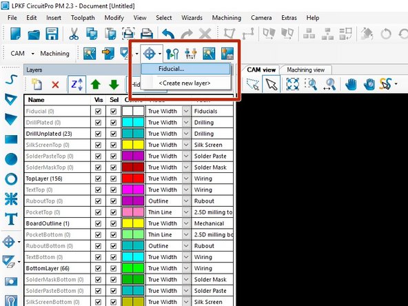
Begin by clicking the Create fiducial button on the toolbar
-
-
-
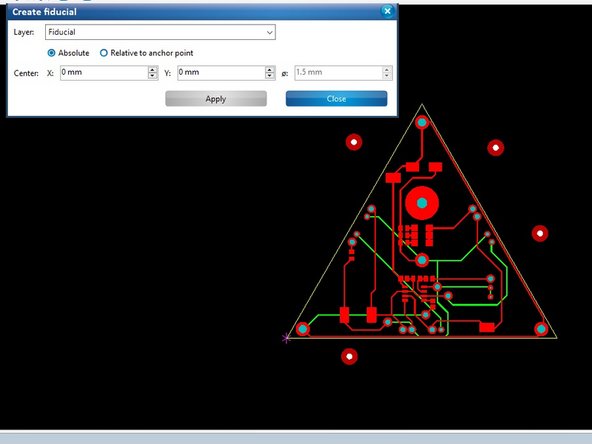
A window will appear which will allow you to enter coordinates for fiducials. Rather than use this method we will directly click on the screen where we wish to place fiducials. Move this window out of the way and click on the black background surrounding your PCB in the areas where you would like to place the fiducials.
-
For the firefly board you should create four fiducials. The fiducials will appear as red circles with white centers.
-
In general, when creating a PCB, you should place the fiducials asymmetrically. This will help avoid misidentification in the following steps. Note that the maximum number of fiducials you may use for any PCB is four.
-
Do not worry about exact placement at this point, we will move the fiducials in the next step.
-
When you are done, click the Close button in the Create fiducial window.
-
It may be helpful to zoom out a little from your PCB. This can be accomplished using a mouse scroll wheel or by using the Zoom tool within CircuitPro.
-
-
-
If you wish to adjust the placement of the fiducials you may do so by zooming in on your PCB by using the Zoom Area button or a mouse scroll wheel. Be sure to change back to the Selection tool (white arrow) when you are done zooming.
-
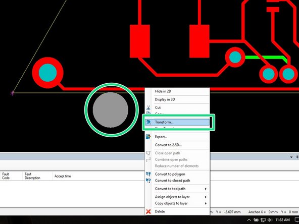
Next, left click and drag your mouse to create a rectangle that entirely encompasses the fiducial. When you let go of the mouse button the fiducial will turn grey.
-
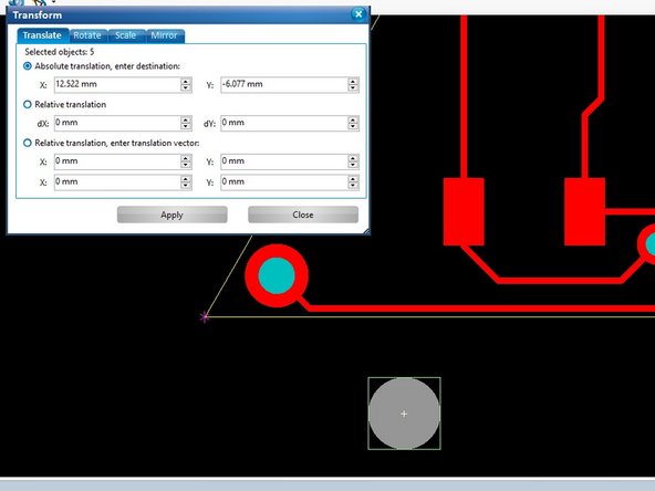
Now right click the fiducial and choose Transform. You may now left click and drag the fiducial where you like. Click Close when you are done.
-
Do not position your fiducials directly against the edge of the PCB. You need to leave room for a tool to route out the PCB at the end of production.
-
Repeat this process for any remaining fiducials you wish to move.
-
When you are done your fiducial spacing should look like that provided in the example above in Step 16.
-
-
-
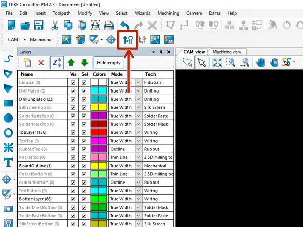
Now you need to create isolation channels around all of your copper traces and pads, drill holes, and define a path to route (cut) out your board. Begin by clicking the Technology Dialog button in the toolbar.
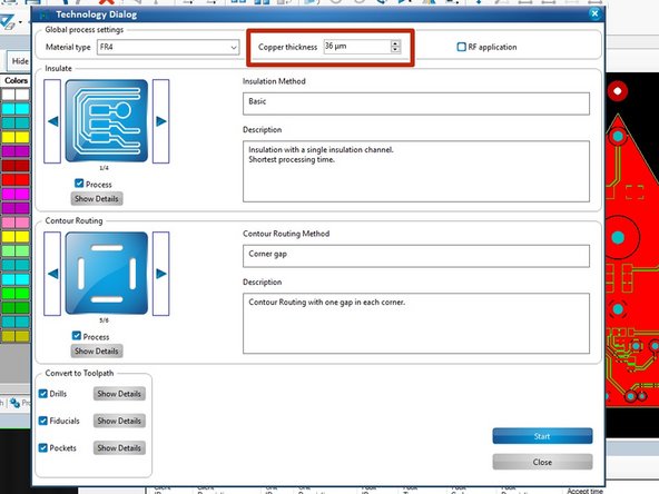
-
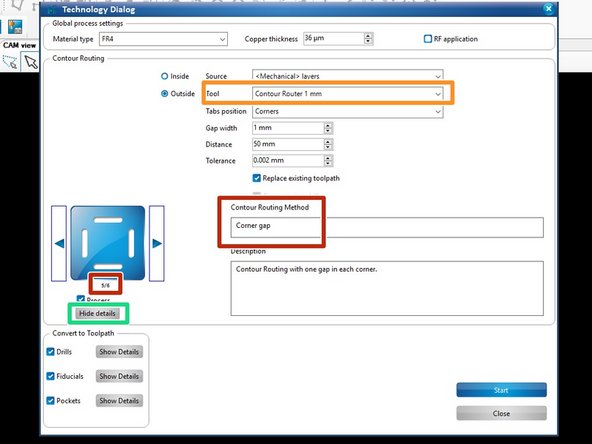
In the Technology Dialog box that appears, change the Copper thickness to 36 μm. This corresponds to the 1 oz/ft^2 copper clad we use in the Maker-E.
-
-
-
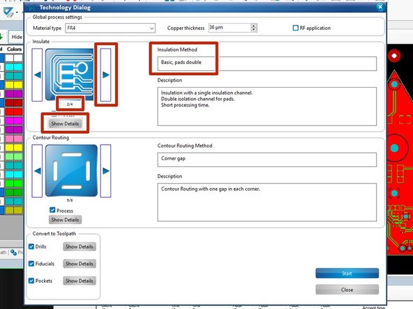
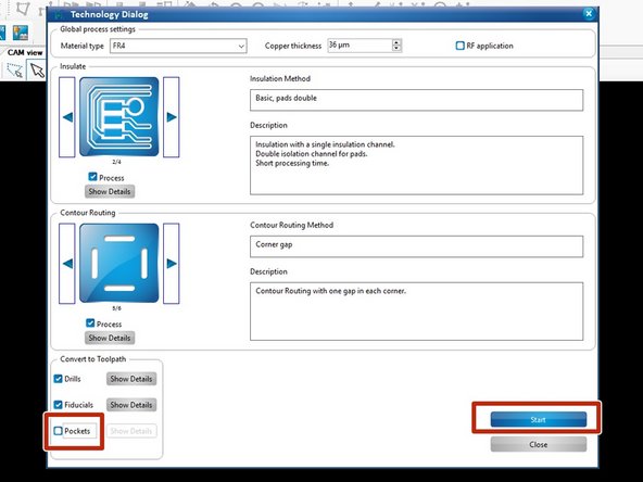
Next, look at the Insulate portion of the window. Click the right arrow button on the screen until the insulation method selected is number 2, Basic, pads double.
-
This method instructs the mill to create isolation channels around everything on your PCB using a single pass of the milling tool and requires additional channels be made around all of your surface mount and through hole pads. These additional channels help to avoid the possibility of solder bridging during the assembly of your PCB.
-
Click on the Show Details button when you are done.
-
-
-
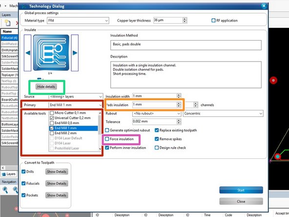
In the Details pane, change the Primary tool from the default Universal Cutter 0,2 mm to End Mill 1 mm.
-
Uncheck the box next to Micro Cutter 0,1 mm. This will prevent the software from using the 0.1 mm milling tool during the mill process. These tools are very expensive and are only required for very specific purposes.
-
You should also increase the Pads insulation value to 1 mm, particularly if this is your first time using the mill. This parameter determines the amount of isolation (ie the amount of copper removed) around the pads where components will be soldered. Again, this extra isolation helps prevent solder bridging.
-
Be sure to uncheck the box for Force insulation. This will prioritize your copper pads and traces and prevent the mill from removing your intended copper.
-
When you are done, click Hide details to display Contour Routing options.
-
Note that if you have power planes in your design you may need to make adjustments to your Ultiboard file to allow for larger pad insulation values. See the PCB Design Tutorial for details.
-
-
-
In previous versions of this tutorial you were asked to change the Contour Routing method from the default. This step has changed. You should now leave the default method of Contour gap which is method 5/6. This will leave your PCB minimally attached to the copper clad and prevent it from lifting during routing.
-
Next, click Show Details and change the routing tool from Contour Router 2 mm to Contour Router 1 mm.
-
When finished, click the Hide Details button.
-
-
-
Uncheck the box next to Pockets at the bottom of the Technology Dialog window. Then click Start.
-
-
-
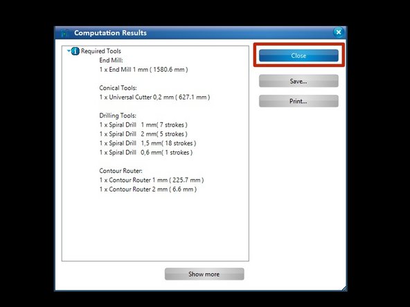
A window will appear detailing all of the tools required to create your PCB. Confirm that the 0.1 Universal Cutter is not in the list of Required Tools.
-
If the 0.1 Universal Cutter is listed as a required tool, you should go back to the Defining tool paths step and disable this tool.
-
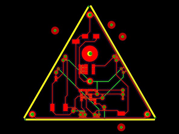
After confirming the 0.1 Universal Cutter is not included in the required tools list, click the Close button. You will now see the toolpaths superimposed on top of your PCB.
-
If the contour router (thick yellow line) overlaps with any of your fiducials, you should move your fiducials out of the path and repeat the tool path generation process.
-
-
-
At this point in time you should take a long pause and check your work carefully. If anything on the board design is wrong at this point you will waste hours of your time in the future.
-
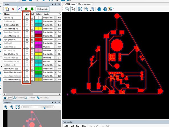
By unchecking the boxes in the Vis column within the Layers window you can turn on and off layer visibility.
-
Disable visibility of all layers, except the top layer and make sure what you see in CircuitPro matches your Ultiboard design. Note that the thin purple and red lines are the tool paths the mill will take to isolate your copper pads and traces. You can ignore these tool paths.
-
Do the same for the bottom layer before you go any further.
-
-
-
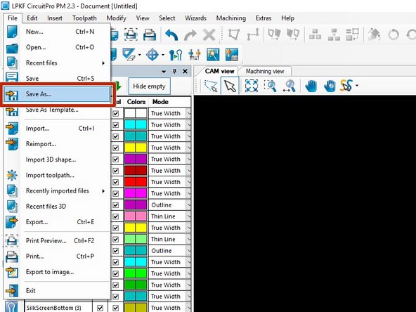
You have now successfully defined all of the toolpaths necessary to mill your PCB. Save your work as a .cbf file.
-
It is recommended that you save your file to your Bucknell netspace so that you can modify it later, if necessary.
-
-
-
Prior to using the PCB mill you must submit your .cbf file to the Lab Director for review. This step will help ensure the success of your mill job.
-
You can contact Matt Lamparter, ECE Lab Director and manager of the Maker-E, at mlampart@bucknell.edu
-
Please attach your .cbf file to the email, along with some details about why you are interested in using the mill (eg. personal project, required course, etc.).
-
You may not continue with Part 2 of this tutorial until the Lab Director has approved your file.
-
-
-
Once you have saved your .cbf file to Netspace you will also need to save it to physical media.
-
As the PCB mill computer is not connected to the internet or the Bucknell network, you will need to use physical media to transfer your .cbf file to the mill computer.
-
A USB flash drive is provided by the mill computer for your use. You are also welcome to use your own media if you wish.
-
Google Drive, Dropbox, Bucknell's netspace, and other internet services will not be accessible from the mill computer.
-
-
-
Once you have your .cbf file saved to physical media it is time to move on to the PCB mill in the Maker-E.
-
Follow part 2 of the tutorial to begin the milling process.
-


Cancel: I did not complete this guide.
14 other people completed this guide.