
Introduction
Published by Matt P. Lamparter with contributions from Owen Meng, Ryder R. Nance and Jacquelyn V. Scott.
-
-
As the PCB mill computer is not connected to the internet, a tablet is provided at the mill station.
-
The tablet has the Dozuki app installed. Users are encouraged to use the Dozuki app to view the PCB mill tutorial.
-
Begin by launching the Dozuki app.
-
Within the app, search for and click on "Bucknell Makers."
-
You will need to authenticate with your Bucknell credentials.
-
Within the app you can navigate to the PCB mill tutorial.
-
-
-
In order to control the mill you will use a piece of software called CircuitPro. This is the same software you used previously to define toolpaths for the removal of copper in order to create a physical representation of the connections needed to complete a circuit.
-
When the mill is actively operating (drilling, milling, routing, or otherwise moving) DO NOT USE ANY OTHER SOFTWARE ON THE COMPUTER. Using multiple applications on the mill computer while the mill is operating can cause the mill to freeze or crash, potentially causing your milling job to fail.
-
The mill was not designed to be used in a networked environment. Consequently, the mill computer is not connected to the Bucknell network or the internet.
-
The mill intentionally lacks a scroll wheel mouse. This is to prevent improper tool assignment. DO NOT USE A SCROLL WHEEL MOUSE WITH THE MILL COMPUTER.
-
-
-
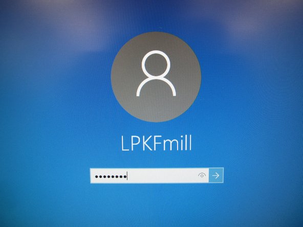
Since the mill computer is not connected to the network you cannot use your Bucknell credentials to log in. Instead, please use the following credentials:
-
Username: .\LPKFmill (note the .\ are required to properly log in)
-
Password: BucknellMakers2019
-
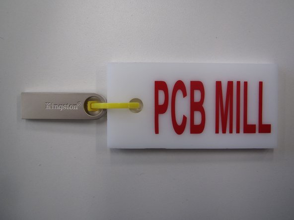
Obtain the PCB Mill training card from a Maker-E technician. Insert the card into the badging box and wait until the box lights up green.
-
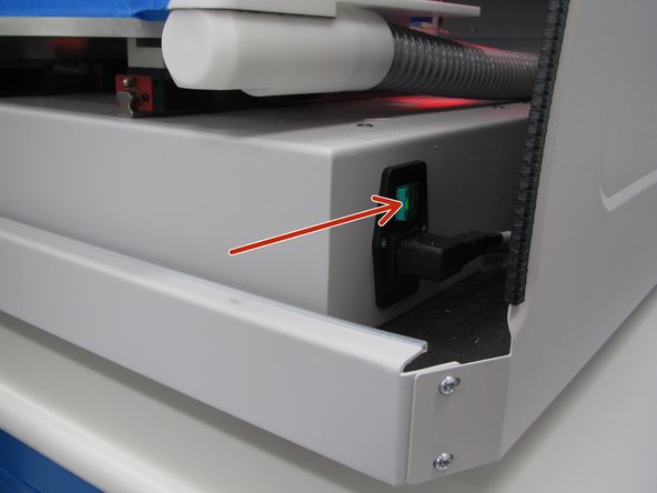
Now turn on the mill. Lift the lid and look at the bottom right side. Press the green power rocker switch. Be sure to close the cover when you are done.
-
-
-
In order to access the .cbf file you created in the previous tutorial you will need to transfer it to the mill computer via the supplied USB drive, or provide your own media.
-
Please use the USB hub below the computer monitor. Avoid using the USB ports on the front of the computer to prevent damage to these ports.
-
-
-
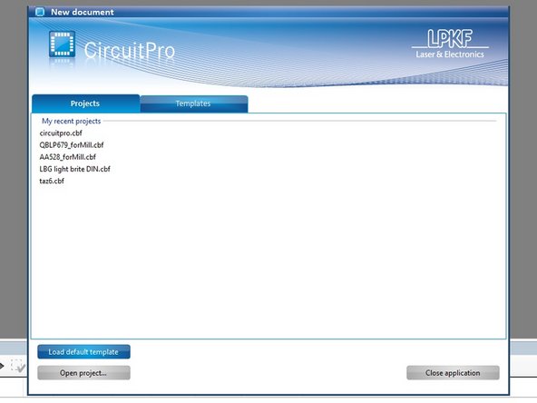
Launch the CircuitPro application. A shortcut should be on the desktop.
-
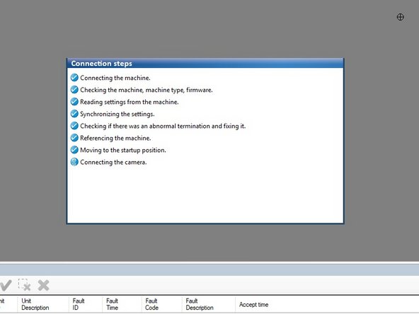
At this point the STATUS light on the mill should turn blue, the milling head should move in all three axes as the limits are located, and then it should move to the back right corner of the bed.
-
Confirm that all of the Connection Steps complete successfully and you are left with the New document screen.
-
If the machine fails to startup properly and you receive any sort of warning message, stop and contact a technician immediately.
-
-
-
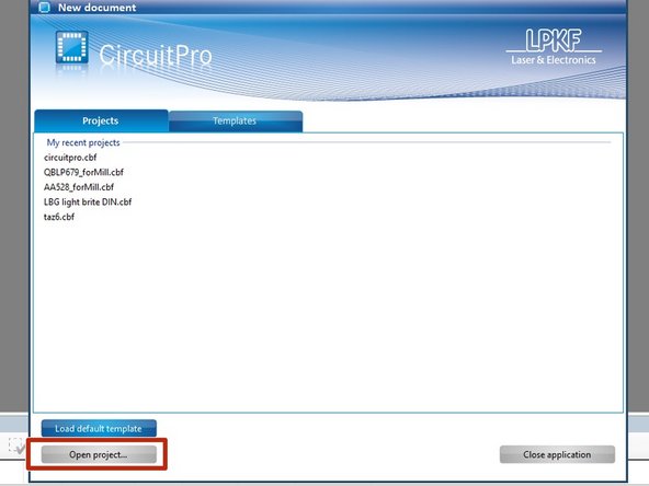
Click the Open project button and navigate to the .cbf file you saved in the previous tutorial.
-
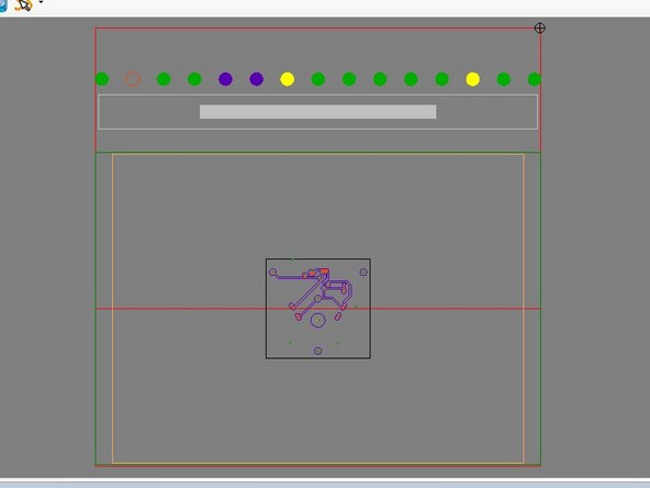
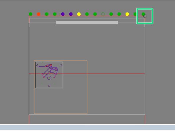
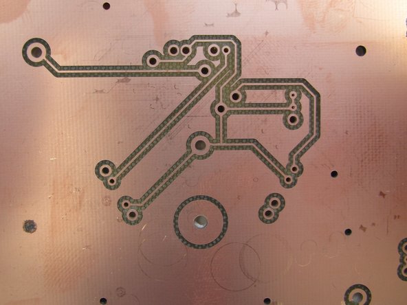
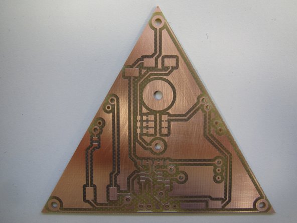
Your PCB design should appear similar to the example shown here.
-
-
-
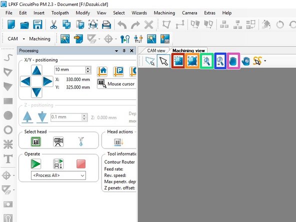
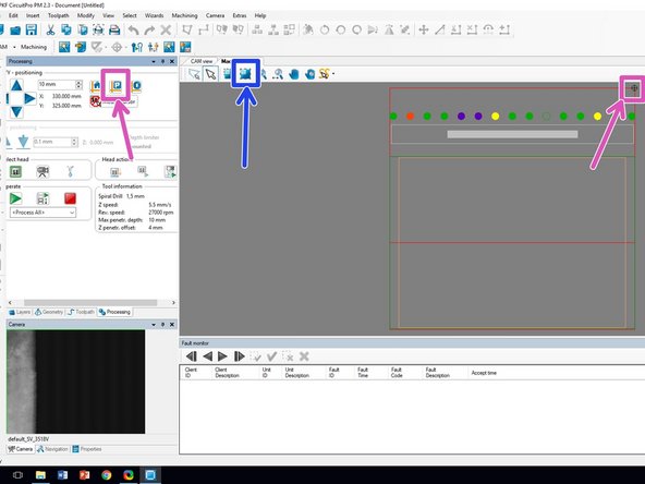
Because the mill computer lacks a scroll wheel mouse, navigation within the PCB window can be difficult. Use the buttons highlighted here to navigate.
-
Use the Fit all job data button to zoom in and view your entire PCB.
-
Use the Fit all machine area button to zoom out and see the entire machine bed and where your PCB will be placed.
-
Use the Zoom Area button to left click and drag a box around a specific area you wish to zoom in on.
-
Use the Zoom button to accomplish the same functionality that a scroll wheel would provide. Left click and drag left to zoom out, left click and drag right to zoom in.
-
Use the Pan button to move your view around the window. With this button enabled, left click and drag to move your view window.
-
Users are encouraged to try all five of these navigation tools before proceeding to gain familiarity with navigating around your PCB.
-
-
-
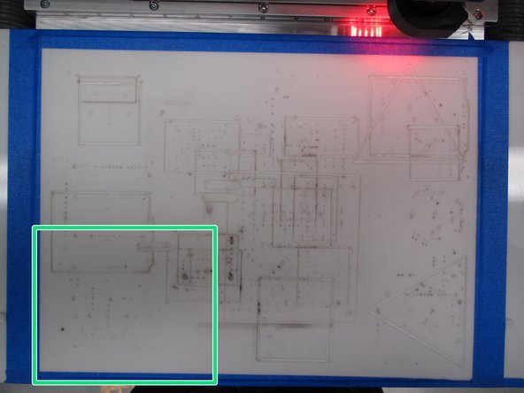
In order to achieve proper vacuum, the milling bed should be clear of all debris and dust.
-
Lift the lid of the mill and remove any copper clad material or orange plastic shim stock. Set this material aside. The white bed should be completely empty. Do not remove the blue tape around the perimeter of the bed.
-
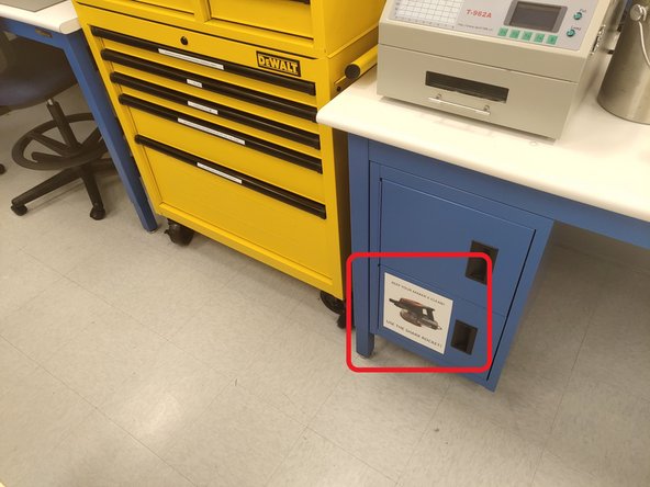
Get the vacuum from the cabinet to the right of the yellow DeWalt tool chest. Use the vacuum to thoroughly clean the white milling bed surface.
-
Return the vacuum when you are done!
-
-
-
In order to use the mill camera for fiducial alignment, it must be calibrated before each milling job. Find a sacrificial piece of copper clad in the drawer below the mill. Use a piece that has already had several boards cut from it.
-
This piece of copper clad will accept a drill hole and then allow the camera to find and calibrate relative to this hole.
-
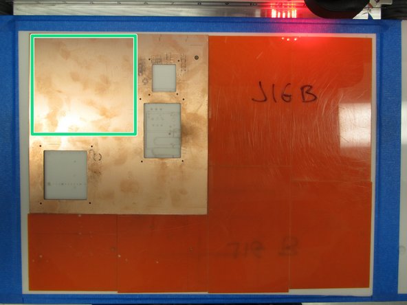
Place the copper in the bottom left corner of the mill bed. This is the area where the mill will operate for calibration. Using the blue tape in the top mill drawer, place two strips across the top and right sides of the copper clad.
-
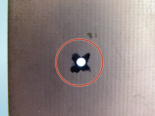
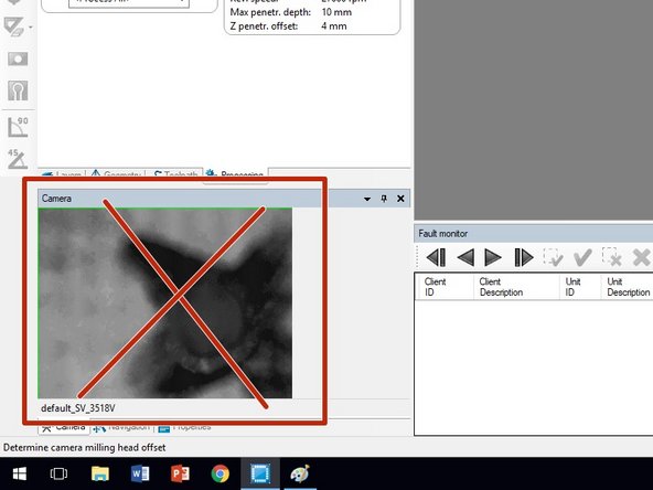
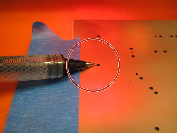
If there are existing holes near the bottom left corner of the copper clad, use the marker in the PCB mill drawer to draw a small X over these holes. This will prevent confusion with any new holes drilled during the calibration process.
-
-
-
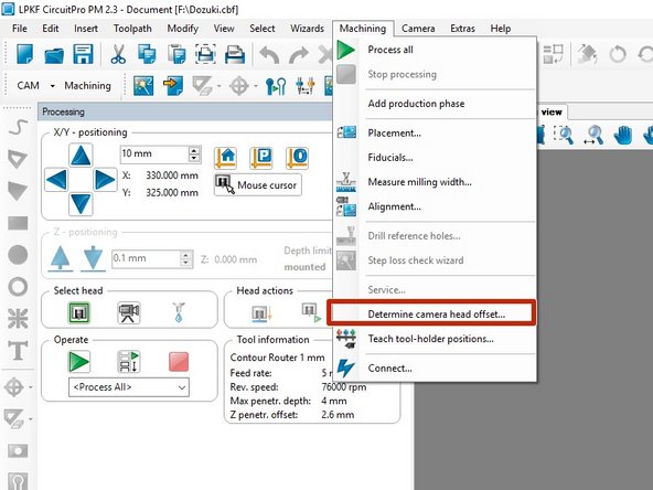
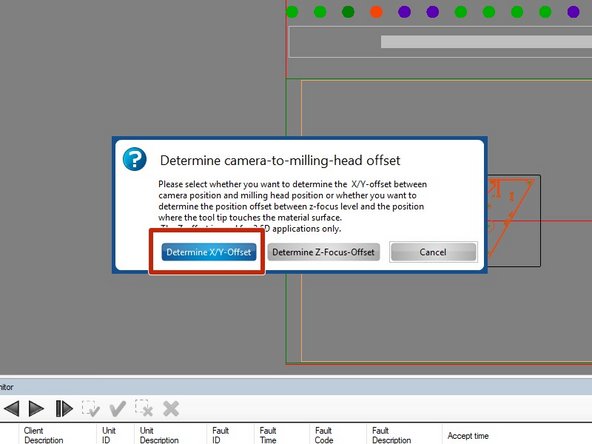
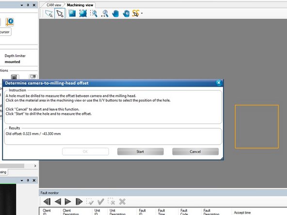
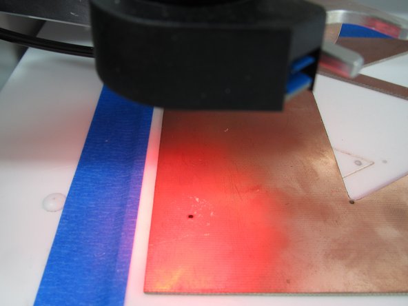
With the copper taped down, close the lid to the mill. Within CircuitPro click on Machining and Determine camera head offset.
-
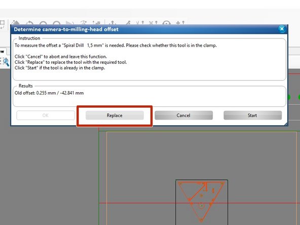
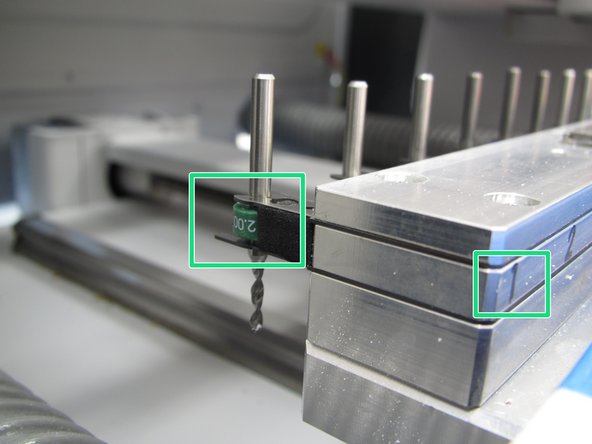
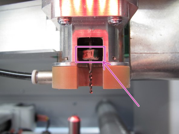
In the next window, click Determine X/Y Offset. If the 1.5mm drill bit is not currenlty in the collet (typical), you will be prompted to replace the current tool with the 1.5mm drill bit. Click Replace.
-
The mill head will now move to the toolbar, remove the existing tool from the collet, and pick up the 1.5mm drill bit and check the drill depth.
-
-
-
The next several steps can be confusing. There is a video summary of the proceeding several steps further on in this tutorial.
-
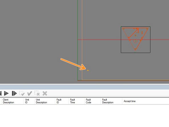
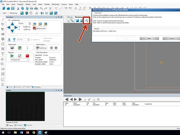
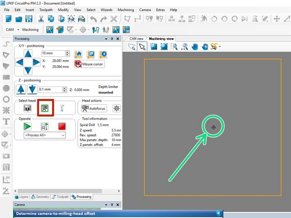
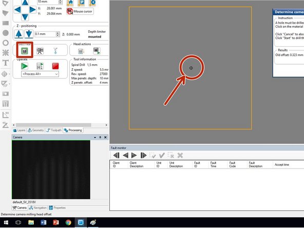
You now need to move the milling head to within the bounds defined on the computer screen as a tiny orange box in the bottom left corner of the mill bed.
-
Click the Zoom Area button, then click and drag a box around the small orange square. This will zoom in on the square and make it easier to position the mill head.
-
-
-
Be sure to zoom in as far as possible, while keeping the orange bounding box visible on the screen. This will help you to precisely position the camera head. You may wish to use the Zoom area tool a second time to zoom in further.
-
Now, click the Camera head button to enable movement relative to the camera head.
-
Finally, click in the center of the orange square. You should see the black cross hairs appear where you clicked.
-
This will move the camera within the bounds of the orange square which is the position needed for camera alignment. Try to position the camera head as close to the center as possible. This will help ensure proper alignment between top and bottom layers.
-
-
-
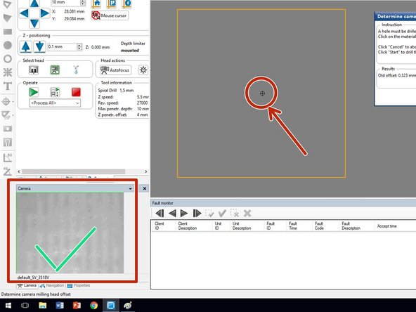
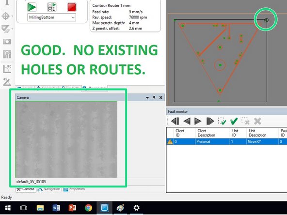
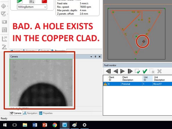
Confirm that the cross hairs are now within the orange square. Examine the output of the camera within CircuitPro. Make sure that the camera shows a light background and no existing holes. This means the camera head is directly over the copper clad board and the area is free of defects.
-
If the camera output displays anything other than a uniform, light colored background while the crosshairs are in the orange box, it means that the camera is looking at a part of the copper clad that is not ideal: pre-existing drill holes or routes, a board edge, or no board at all.
-
If the camera displays a non-ideal area you need to move the copper clad. Lift the mill lid, peel up the blue tape and adjust the copper clad, paying attention to the camera display. Move the copper clad slowly until the camera displays a light, uniform area, free of drill holes and routes.
-
Once you are satisfied with the camera output, remember to tape down the board again and close the mill lid.
-
-
-
You now need to switch control from the camera head to the mill head. Click on the mill head button. You should hear the mill head move slightly, but the cross hairs should remain in the orange box.
-
Note that the camera display will change. This is because the camera head is now looking at a different portion of the bed. This is normal and can be ignored, as long as you confirmed a good camera output in the previous step.
-
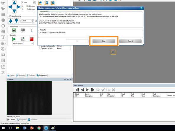
Once you have confirmed that you are controlling the mill head and the cross hairs are in the orange box, click the Start button to begin drilling your alignment hole.
-
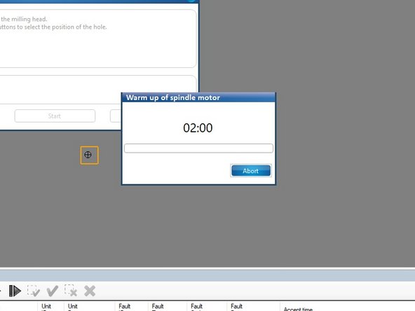
If this is the first time the mill has been operated in awhile it will need to warm up the spindle motor for 2:00 minutes prior to operating.
-
-
-
This video summarizes the last several steps of zooming in on the orange box and then switching between the two heads.
-
When you are done with this step:
-
Confirm your cross hairs are in the center of the orange box
-
Confirm you have switched to the milling head
-
Press the Start button
-
-
-
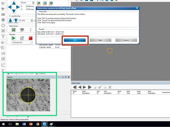
After two minutes have elapsed the mill will drill a 1.5mm hole, move the camera head to view the drill hole, and focus the camera.
-
After focusing, a window will pop up asking you to agree to the suggested offset. First, confirm that the camera display shows a black hole encompassed by a yellow circle, centered within cross hairs as shown in this example.
-
If the camera display looks good, click OK to confirm the camera alignment. Click Save in the next window to transfer these settings to the mill.
-
When you are done, click the Fit All button to zoom out.
-
Finally, click the P button to move the head to the "Park" position which will allow you to safely remove the scrap copper clad.
-
After the head has finished moving you may lift the mill lid and remove the copper clad and tape you just used.
-
-
-
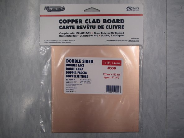
You now need to add copper clad material to the milling bed for your PCB milling job.
-
Examine the piece you used in the previous step, as well as any previously used pieces in the top drawer of the milling bench.
-
Look for a piece of copper clad with enough room to accommodate your PCB design plus the fiducial holes you added to your design. Having a 1:1 printout of your PCB (plus fiducials) on paper can aid in identifying whether your design will fit on a piece of copper clad.
-
Examine BOTH SIDES of the copper clad material. It is possible that there are milling channels on one side of the material and not the other. Attempting to mill your PCB where existing holes or isolation channels already exist may render your board unusable.
-
If no current piece will accommodate your design, you may open a new piece of copper clad located in the same drawer.
-
Try to be conscious of other Maker-E users when using the copper clad material. Do not simply use a new piece of copper clad material because it is available. You should always use a piece of copper clad with existing routes whenever possible.
-
As a general rule it is time to use a new piece of copper clad if approximately 50% of the surface area of the existing material has been routed (cut out). Three firefly PCBs can be routed from a single piece of copper clad.
-
-
-
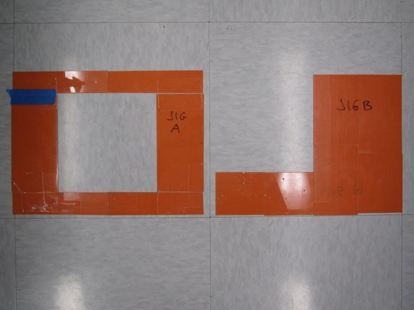
Locate the two jigs, A and B, in the drawer below the mill. The jigs are used to cover the excess space on the vacuum bed which is not covered by the copper clad. This increases the pressure on the copper clad and prevents it from moving during milling.
-
Choose between jig A and B based upon the state of the white milling bed surface:
-
Use jig A - if the center of the milling bed is relatively free of holes and routes while the outer edges have lots of holes and routes.
-
Use jig B - if the center of the milling bed has lots of holes and routes while one of the outer edges is relatively free of holes and routes. Note that jig B can be oriented in four different ways to accommodate the four corners of the bed.
-
-
-
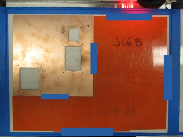
Place the jig within the bounds of the blue tape around the edges of the mill bed, then place your copper clad inside the jig.
-
Add some blue tape to adhere the copper clad to the jig, and to adhere the jig to the mill bed. Keep the tape away from where the mill will be fabricating your PCB, as having tape in the way can interfere with proper milling.
-
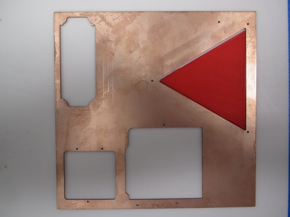
If the copper clad you chose had a firefly board previously routed from it, be sure to use one of the plastic 3D printed triangles in the mill drawer to fill in this hole.
-
Close the lid when you are done.
-
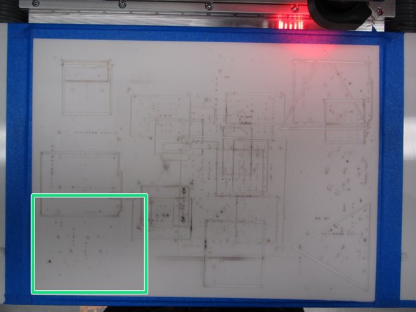
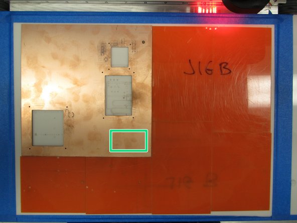
Note that in this example the copper and jig were placed in the top left corner, while the bottom left corner was highlighted in green as the optimal location. Because the milling process involves flipping the board about an imaginary horizontal axis, we begin the milling process in the "mirror" location about this axis. More on this later.
-
-
-
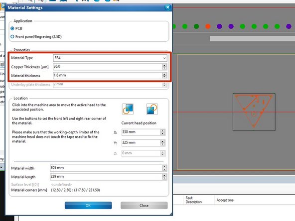
Return to CircuitPro and define the type and thickness of material you will use. Choose Edit -> Material settings from the menu bar. Confirm that:
-
Material type is FR4
-
Copper Thickness is 36 μm
-
Material thickness is 1.6 mm
-
-
-
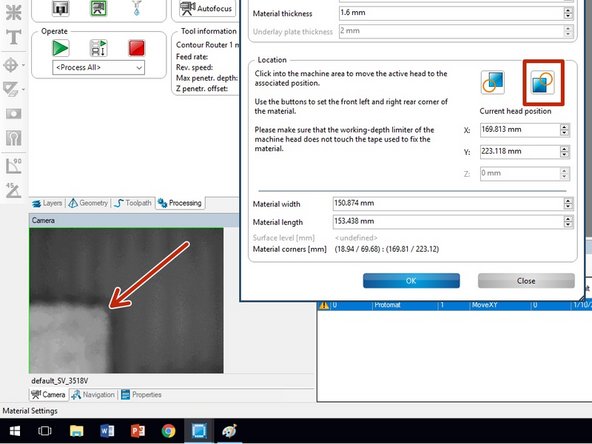
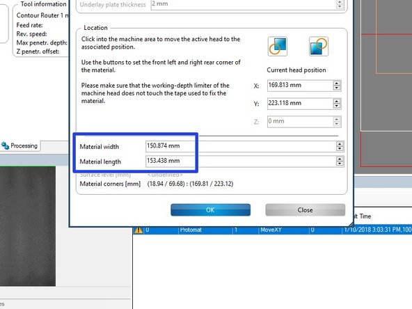
With the copper in place it is necessary to define the bounds of your material in the milling software. The green rectangle in the Machining view represents the entire mill bed. The orange rectangle is where CircuitPro assumes the bounds of your copper clad are located. These bounds must be updated to represent the copper you just placed.
-
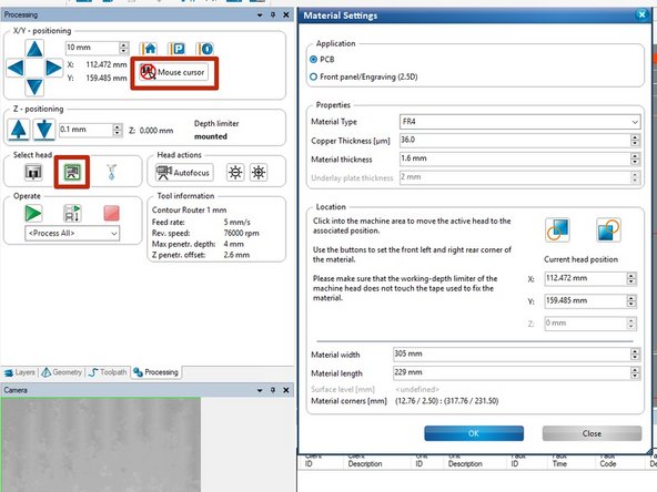
With the Material Settings window still open, move it to the right so that the Processing window can be seen.
-
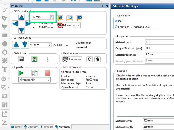
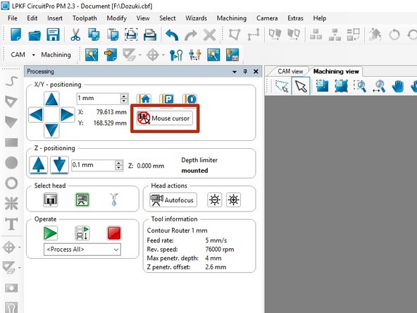
Within the Processing window, click on the Camera head button. Ensure that the Mouse cursor button has a red cross mark across it. This will allow us to click on the milling bed on the screen and move the camera head around to locate the boundaries of the copper clad.
-
-
-
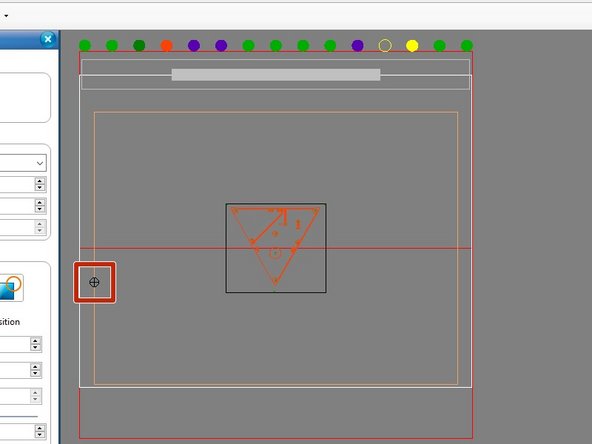
You now need to set the locations of the lower left corner and upper right corner of your copper clad board so the mill knows where to operate. Move the Material Settings window so that you can see the entire milling bed.
-
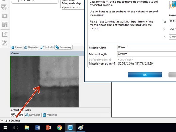
Look at the milling bed within the Machinig view tab. Left click on the bed where you believe the bottom left corner of the copper clad is located. In this example this will be on the far left edge of the milling bed, slightly below the red line running across the middle. Notice that the circular cross hairs have moved to where you clicked.
-
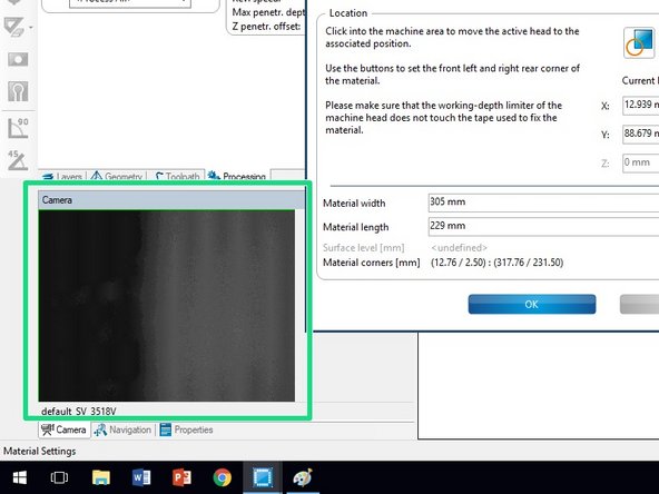
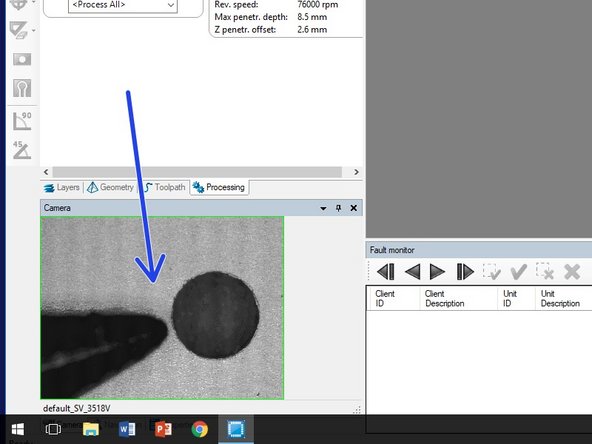
The milling head will now move and the camera display will update to show you where the head is located. The image will be out of focus.
-
-
-
The idea here is to move the camera head around until it sees the bottom left corner of the copper clad material.
-
Begin by locating at least one edge of the copper clad. Looking through the lid at the mill bed and the copper clad can be helpful in determining which direction to move the camera. The copper clad will appear on the screen as nearly white, while the shim stock and white mill bed will appear darker.
-
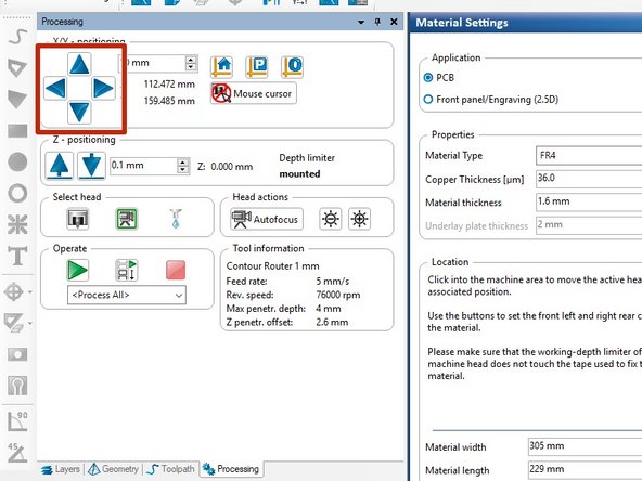
Once you have a rough idea of where the bottom left corner is you can more precisely move the camera head using the X/Y positioning controls in the Processing window.
-
Set the movement increment to where you want it and then use the four arrow keys to move the head.
-
-
-
Try to position the bottom left corner of the copper clad in the center of the camera display. Do not worry that the image is out of focus.
-
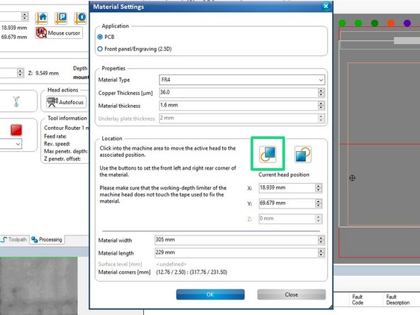
When you are happy with the location, click on the button in the Material Settings window to lock in the bottom left corner.
-
You should see the Machining view window update and the orange rectangle should now properly represent where the bottom left corner of the copper clad material is located on the milling bed.
-
-
-
Repeat the previous few steps to locate the top right corner of the copper clad material. When you have the corner in the center of the camera display, click on the corresponding button in the Material Settings window.
-
The Machining view window should now properly display the bounds of the copper clad material as represented by the orange box.
-
Confirm that the dimensions of the copper clad board are within a few millimeters of 152mm x 152mm, which corresponds to the 6" x 6" boards used in the Maker-E. If your dimensions are significantly off, repeat the last few steps or ask a technician for help.
-
When you are satisfied with the bounds of the copper clad, click OK in the Material settings window.
-
Do not worry if your PCB falls outside this bounding box. We will move it shortly.
-
-
-
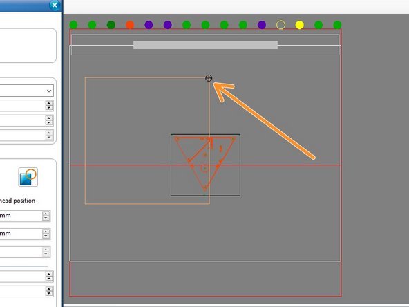
Next, you need to position your PCB on the copper clad material. If the material is new you do not need to worry about overlapping with previously milled PCBs. If the copper clad material has been used previously, you will need to carefully position your PCB so as not to overlap with any existing holes, routes, etc. on the copper clad material.
-
Begin by choosing Machining -> Placement from the CircuitPro toolbar. Now you can click and drag your PCB in the Machining view window to position it. Be sure to stay within the orange bounds of the copper clad, and do not overlap with previous routes.
-
Note that you can also rotate your PCB which may help position it among holes left from other PCBs which have already been routed.
-
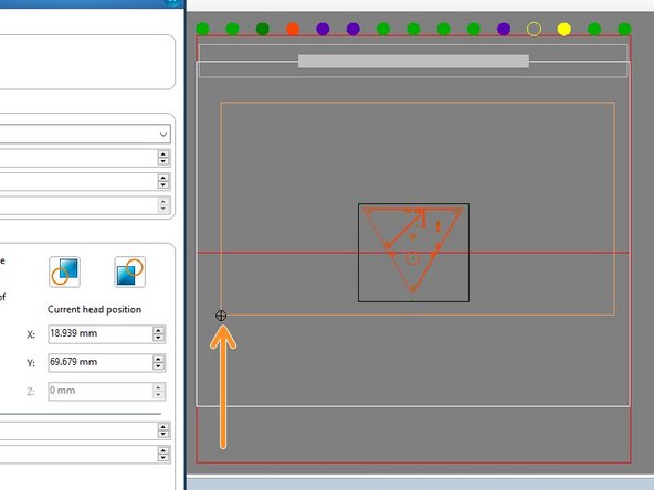
Notice how in this example the four green fiducial holes lie well within the orange copper bounding box in the Machining view.
-
The PCB has been placed in the top left corner in the Machining view to correspond with the available space in the copper clad material, highlighted here in green.
-
-
-
As CircuitPro does not display previous routes in the Machining view it will be necessary to take control of the camera head again and move the head around the copper clad to ensure your PCB placement will not interfere with any existing routes or holes.
-
Click Close in the Placement window, then make sure that the Mouse cursor button has a red slash mark across it to enable moving the camera head.
-
Within the Machining view, left mouse click at several locations around the borders of your PCB (you can ignore the black box surrounding it). Wait for the mill head to move to the location you clicked and watch the Camera display. Confirm that there are no existing routes, holes, etc. on the copper clad where your PCB is placed.
-
If the Camera display shows an existing hole or route where your PCB is placed you will need to adjust placement. Go back to Machining -> Placement to make these adjustments. Then move the head again and confirm, using the camera, that you have avoided the existing holes or routes.
-
-
-
When you are satisfied with your PCB placement, be sure to close the Placement window.
-
Move the head out of the way for future inspection. Do this by clicking the P button again to move the mill head to the park position.
-
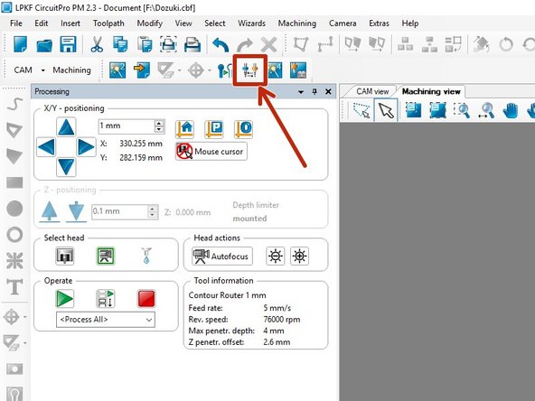
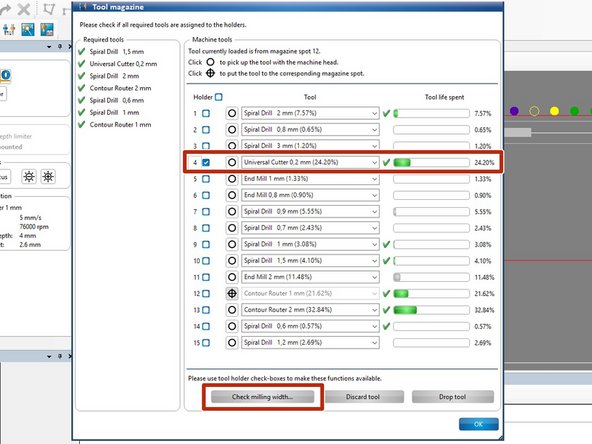
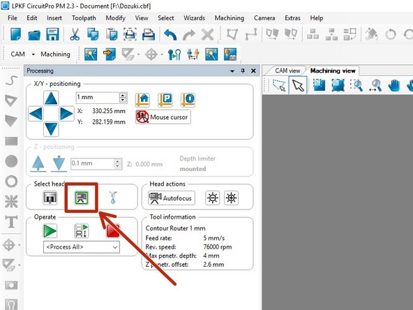
Now we need to confirm we have all of the bits required for the mill process. All of the bits required for the firefly PCB should already be loaded in the PCB mill. If you are milling a board that requires tools not already loaded, please see the Lab Director or a Maker-E tech.
-
Click on the Tool magazine button.
-
-
-
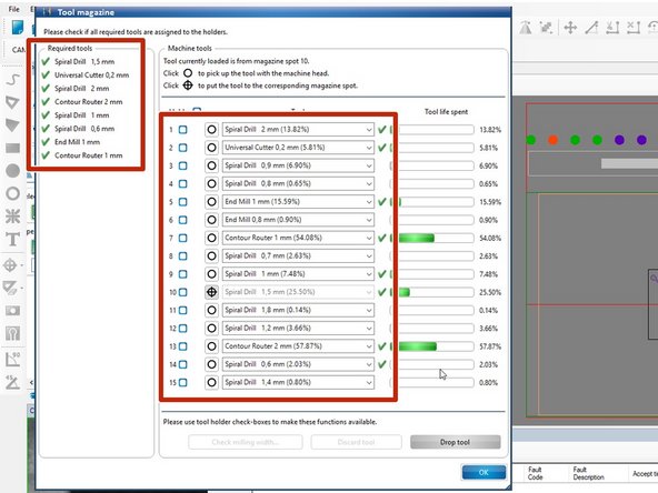
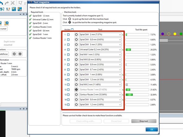
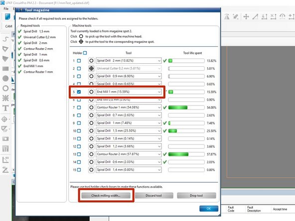
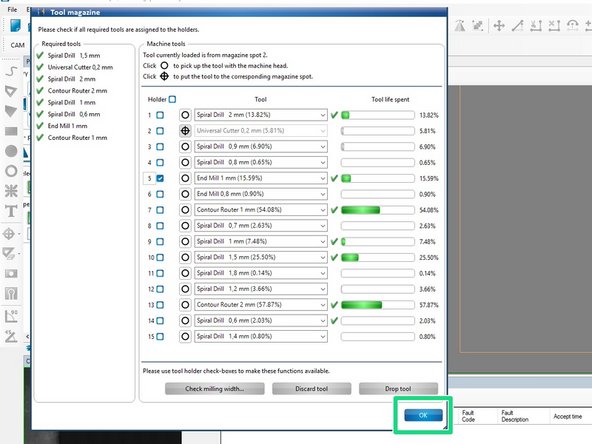
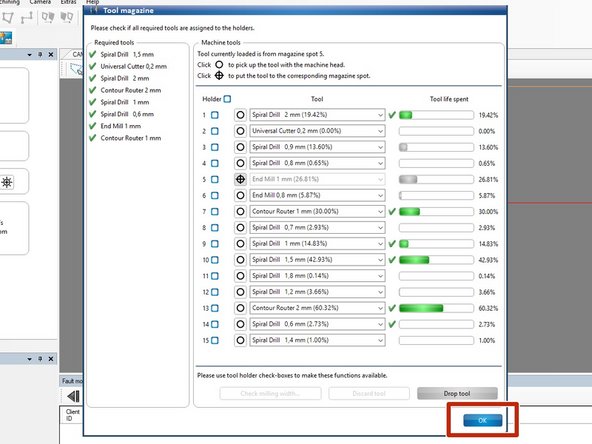
The Tool magazine window uses the Required tools panel on the left to list which bits are required for the milling process of your PCB. Any bits with a green check mark are already loaded in the mill tool holder. Any bits with a red x need to be loaded in the tool holder.
-
Again, if you are milling a firefly PCB all of the tools you need should already be loaded. If you see any red x’s please contact the Lab Director or a Maker-E tech.
-
The Machine tools panel on the right lists the bits which are currently loaded in the mill tool holder, positions 1 through 15. You should confirm that all of the tools in the left panel appear in the right panel.
-
Do not yet click OK. We need to address two more issues in the following steps.
-
-
-
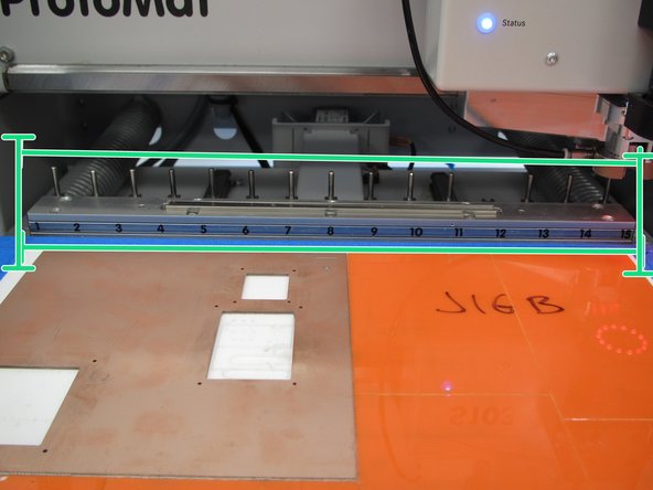
With this window open we need to confirm that the bits loaded in the mill tool holder are correctly assigned in the Tool magazine window. Lift the mill lid and examine the tool holder at the back of the mill. Look at each position, beginning with #1 on the left and working to #15 on the right.
-
Pay attention to the color of the plastic ring around the bit and the number printed on the ring. It may be necessary to spin the bits to see the number. Do not remove the bits from the holders. In general, the colors correspond to the bit type:
-
Green is a drill bit
-
Orange is a universal cutter
-
Purple is an end mill
-
Yellow is a contour router
-
White ringed bits should have a small colored area on the white ring. This color matches to the examples above.
-
Confirm that the bits in the tool holder correspond to what is assigned in the Tool magazine window within CircuitPro. If there are any discrepancies, stop what you are doing and alert a technician.
-
-
-
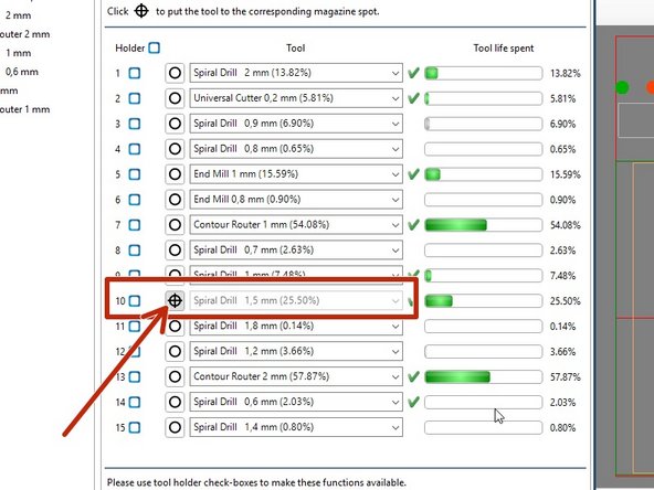
If a tool is missing from positions 1 through 15 in the mill it is most likely in the collet (milling head).
-
Refer to the Tool magazine window and look at the number which corresponds to the position where the tool is missing from within the mill.
-
If you see a cross hair symbol immediately to the right of this number it indicates that the milling head is currently holding this bit.
-
Confirm that the mill is indeed holding this bit.
-
Be sure to close the lid when you are done.
-
-
-
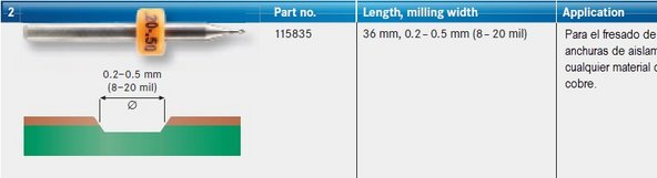
Now we need to calibrate the Universal Cutter 0.2 mm. This tool is used to create small portions of the isolation channels around all of the traces and pads on the PCB. It is a pointed tool, so the deeper it plunges into the material the wider the channel of copper it removes. Check out this nice representation from Midwest Circuit Technology for an explanation.
-
Nominally, this tool should remove a channel of copper which is 0.2 mm wide. To be safe, we will instruct the mill to use a value of 0.25 to give us extra clearance between residual copper and traces.
-
We must calibrate the tool to ensure proper channel width prior to milling our PCB.
-
-
-
To calibrate the universal cutter, check the box next to the tool position number that corresponds to this tool in the Machine tools window. In this example it is number 4. Then click the Check milling width button.
-
-
-
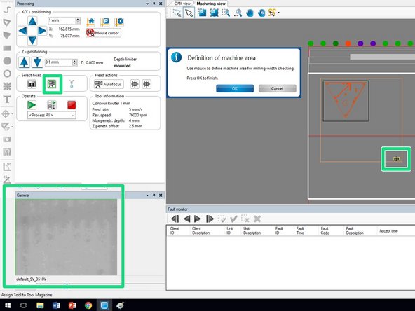
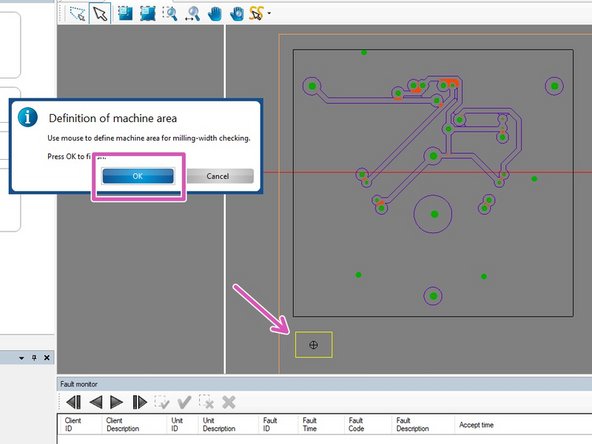
In order to calibrate the milling width of the universal cutter the mill must run a test cut and then check this cut. The first step in this process is to define an area where the test can happen.
-
The proposed area is highlighted in yellow within the bounds of the orange box (the copper clad material). You can move this yellow box by clicking anywhere in the mill bed.
-
Choose a spot that is out of the way, like in a corner or along a board edge. Don’t choose a location that is in the middle of a large blank area that could be used to mill another design; look for a region that is too small for another design.
-
If the copper clad in the mill already has boards and holes cut from it you need to pay attention to the camera display as you try different locations. Choose a location where the copper has not been milled, drilled, or routed. Be sure that you are moving relative to the camera head and not the milling head. Press the camera head button.
-
-
-
After you have clicked on a spot where you would like to test the milling width, confirm that:
-
the yellow box is in the correct location within the orange bounds of the copper clad
-
the camera head is selected
-
the camera display shows a clear space
-
There is no blue tape near where the mill head will operate. If the head moves over the tape during milling it can adversely affect the mill operation.
-
If you are satisfied with the location, click OK to begin the milling test.
-
-
-
Now the mill will exchange tools, pick up the universal milling bit, adjust the depth of the bit, and move into position to mill the test line.
-
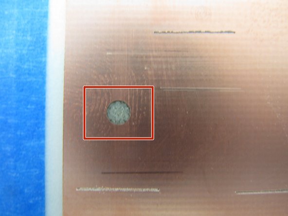
The mill will plunge into the copper, mill a channel that is 10 mm in length, stop the spindle motor, and return to the beginning of the channel to optically inspect the channel.
-
After the camera finishes focusing, confirm that the image looks in-focus and click Yes.
-
-
-
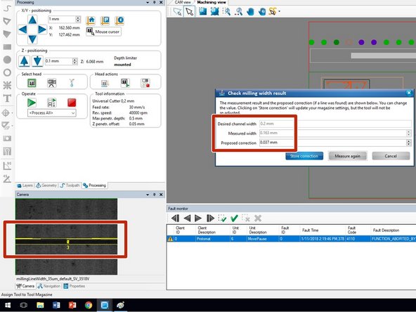
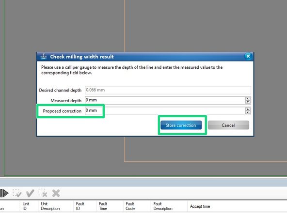
Using the optical data from the camera the mill will automatically determine the width of the milled channel. This value will be reported back, along with a proposed correction.
-
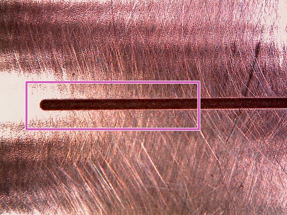
The channel should appear as a thick black line as shown in this example. The proposed correction should be on the order of +/- 0.1mm.
-
If your results deviate from this example significantly, stop and alert the Lab Director or a technician.
-
Be sure to visually inspect the test cut as well. Lift the lid of the mill and examine the cut closely. Try to confirm that the cut went entirely through the copper layer, rather than just scratching it. You should see a clearly defined dark black channel, or possibly a white channel if the FR4 debris is left.
-
-
-
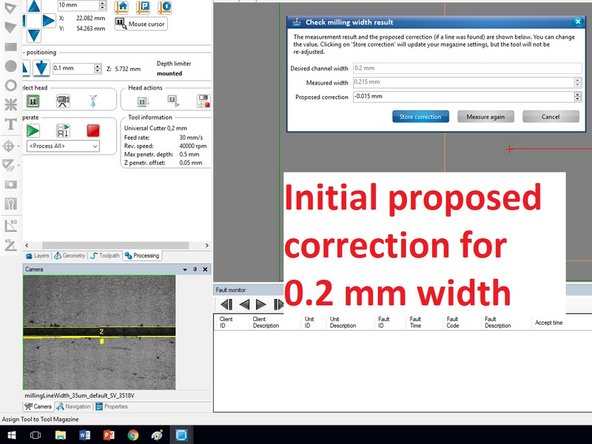
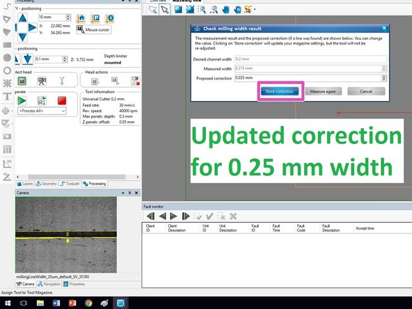
Recall that we want to increase the desired channel width from 0.2 mm to 0.25 mm.
-
The first image here shows a proposed correction factor to get to the channel width of 0.2 mm. In this example the measured width of the milled channel is 0.215 mm, so the software proposes decreasing the width by 0.015 mm, a change of - 0.015 mm. This value was automatically entered by the software.
-
However, we actually want to increase the width to 0.25 mm. This means we need to widen the channel by 0.035 mm beyond the measured value of 0.215 mm. The second image here shows this value which was manually entered.
-
You should take whatever value is shown in the Measured width box for your milled channel and subtract this value from 0.25 mm. Whatever the result is should be entered into the Proposed correction field. Be sure to get the sign correct: negative values decrease width while positive values increase width.
-
When you have entered your correction, click Store correction.
-
Failure to calibrate the universal tool properly will result in a board with many shorts which will ultimately cause your PCB to fail.
-
-
-
Finally, we also need to calibrate the 1 mm end mill used for the majority of insulation on your PCB.
-
Click the checkbox next to the 1 mm End Mill tool. Then click the Check milling width button.
-
You will be asked to choose an appropriate place on your copper clad to perform this test. Follow the same procedure you did for the 0.2 mm universal cutter tool to choose an appropriate area for a test.
-
Once you choose an appropriate area, click OK. The mill will pick up the proper tool and mill a small circle in the location you chose.
-
-
-
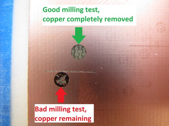
This test is different than that used for the 0.2 mm universal cutter. The 1 mm end mill is a flat end tool so channel width is constant. What we care about is that the tool plunges deep enough to remove all of the copper layer. The camera cannot determine whether all of the copper has been removed so it is left to the user to visually inspect.
-
When the mill finishes operating and the head moves out of the way, lift the lid and visually inspect the circle. It should look like the example shown here. The copper is completely and uniformly removed.
-
If the circle milled during your test does not look like the image (there is copper remaining or the surface is simply scratched instead of completely removed) you will need to increase the depth of this tool. See below.
-
In this example the circle was milled well so we do not need to make any corrections. If your circle was milled well you can leave the proposed correction at 0 mm and click Store correction.
-
If your circle was not milled well, please see the next step.
-
-
-
If your circle was not milled well and still contains some copper you need to tell the software to plunge the tool deeper. Enter a proposed correction of 0.05 mm, then click Store correction. Repeat this test until you get a clean circle with no remaining copper.
-
When you are satisfied with the calibration of both tools, click OK in the Tool magazine window.
-
-
-
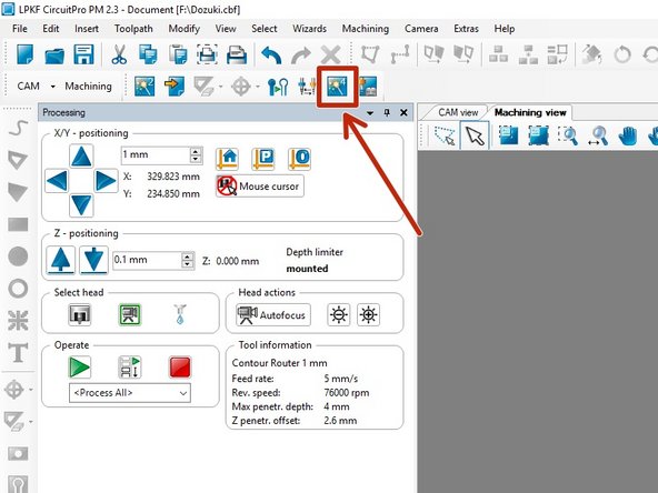
You are now ready to begin milling your PCB. Click the Board production wizard button in the toolbar.
-
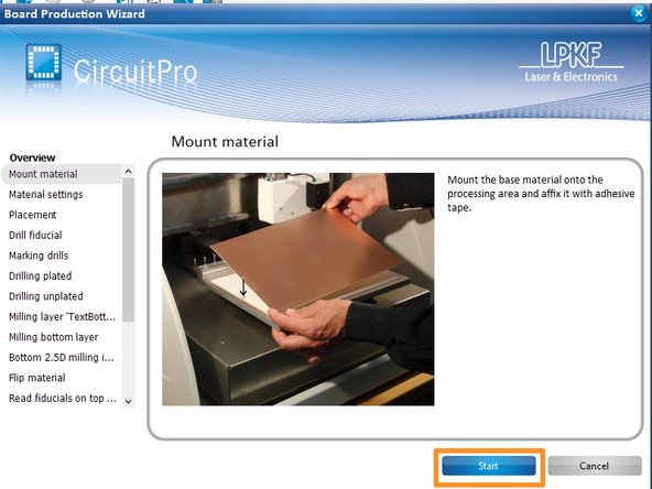
Click Start when prompted by the Board production wizard.
-
-
-
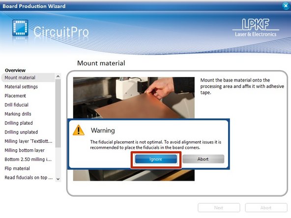
If you experience a warning about "non optimal fiducial alignment" you may safely click Ignore on this warning box.
-
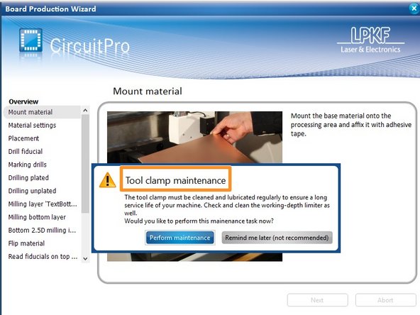
If you receive a warning about Tool clamp maintenance please stop and contact the Lab Director or a Maker-E tech.
-
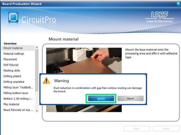
If prompted, choose to Ignore the warning about dust reduction. This simply means that after routing (cutting) out your PCB, the mill will make a second pass along the routing channel in order to clean out debris generated by the routing bit. The LPKF technicians have instructed us to follow this practice.
-
-
-
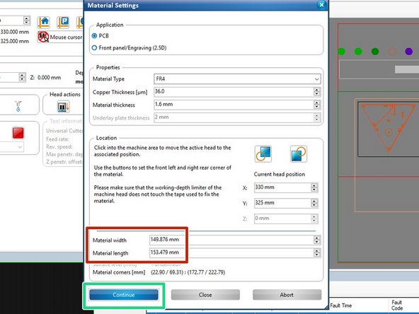
The next window will display material settings. We have already set the material type, copper thickness, material thickness, and location of the copper clad material in previous steps.
-
Make sure that the Material width and Material length are within a couple millimeters of the actual board size (152mm).
-
Confirm that your settings match those in the example, then click Continue.
-
-
-
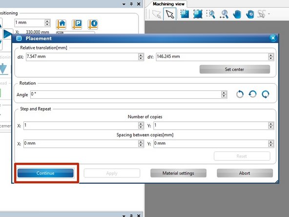
The next window is for placement, which we accomplished in a previous step. Click Continue.
-
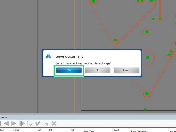
When prompted, choose to save your work to the flash drive.
-
-
-
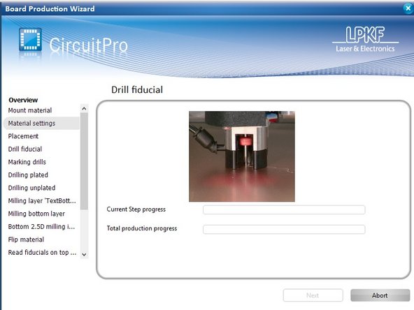
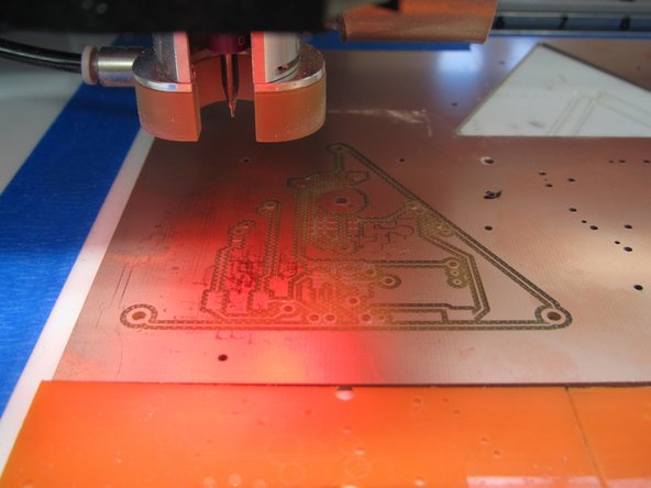
Now the mill will begin to operate. It will begin with the bottom layer of your PCB. The order of operations is as follows:
-
Drill fiducial holes
-
Mill pilot marks for all drill holes
-
Drill remaining holes
-
Mill bottom layer
-
-
-
When all of the above steps have completed the mill will pause and wait for user interaction.
-
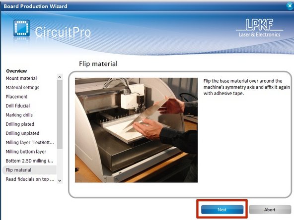
When you see the Flip material screen, it is safe to lift the lid and examine the copper clad to ensure that everything was milled properly. Pay attention to the following:
-
Isolation paths (areas where copper was removed) should appear sharp, clean, and consistent. There should be no burrs, breaks in the path, or missing paths.
-
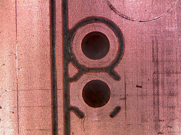
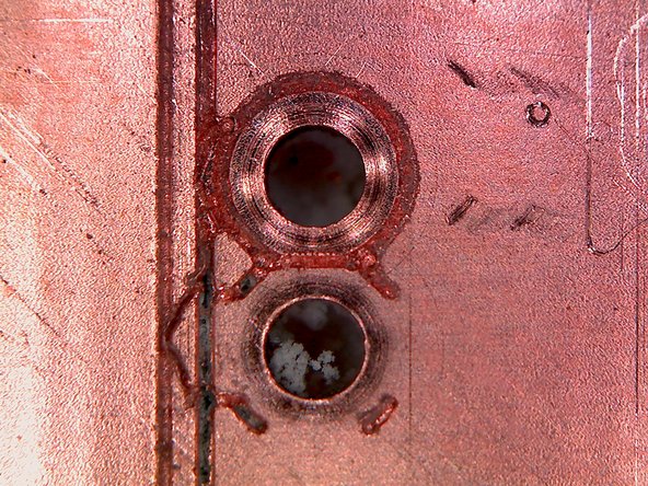
Drill holes should be perfectly aligned within copper pads. Holes should pass completely through the copper clad material.
-
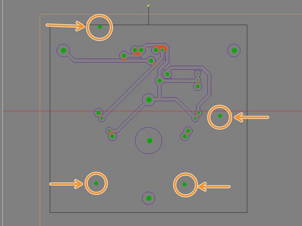
The fiducial holes defined previously should be located around the edges of the PCB.
-
If you notice any problems with these bullet points, please contact the Lab Director before continuing.
-
If you feel the bottom side of your PCB did not mill properly, ask a tech for help. DO NOT AUTOMATICALLY START A NEW PCB. This wastes expensive resources. Typically, a PCB can be routed a second time to correct any issues present after the first pass.
-
-
-
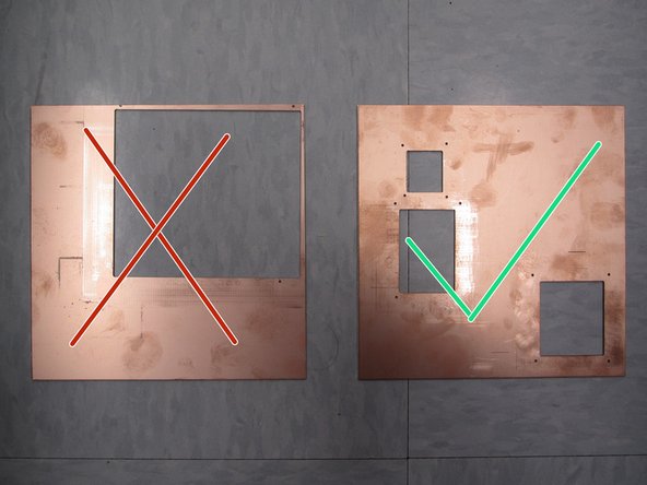
Here are several images of what your PCB should NOT look like. Note the following:
-
Portions of isolation channels are not entirely milled. The channel should be uniformly dark, but instead there is residual copper remaining in the channel. The tool did not cut deep enough.
-
There are copper burs lining many of the isolation channels and around pads. These burs will cause electrical shorts.
-
If you experience these issues, please stop and speak with a Maker-E tech.
-
-
-
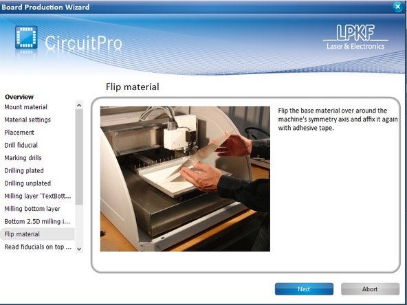
If everything looks good then you need to flip the jig (only jig B needs to be flipped, not jig A) and the copper clad.
-
First remove the tape holding the jig to the bed and the tape holding the copper clad to the jig.
-
Remove the jig and copper clad and set them aside temporarily, paying attention to how they were oriented. While the bed is empty, use the vacuum to once again clean up any debris.
-
Finally, return the jig and copper clad to the bed. When you return the materials they should be flipped about a horizontal axis running through the middle of the bed. Watch the video for an example.
-
Flipping the material in the proper direction is crucial to milling the next side. Be sure to flip the material the right way.
-
Be sure to remove all tape from the jig and copper clad prior to flipping them. Leaving any tape on the side of these materials that sits on the vacuum table will cause milling issues.
-
-
-
After flipping the material, click Next in CircuitPro to continue milling the top side of your PCB.
-
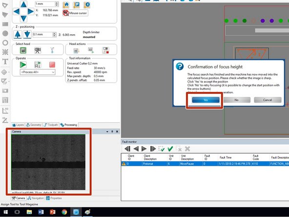
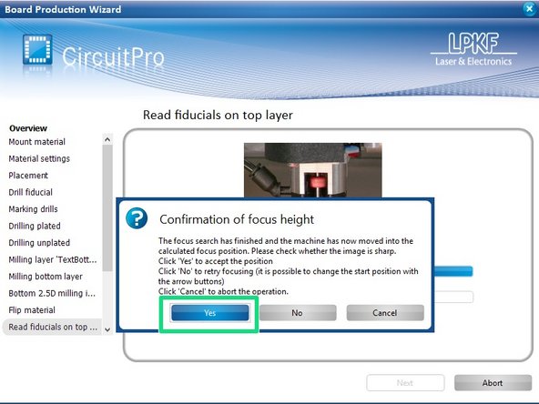
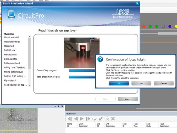
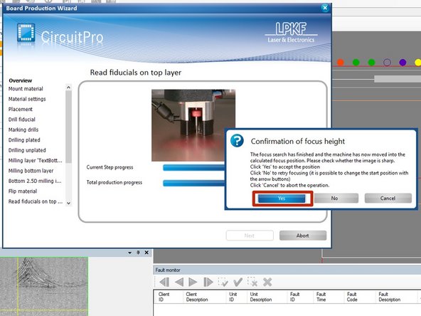
The mill will now search for the fiducial holes around the perimeter of your board. This process begins by moving the camera into position and focusing it. When prompted, click Yes to confirm focus height.
-
-
-
The camera will now begin to search for the first fiducial hole, usually beginning in the bottom left corner. Most likely the search will fail and you will need to move the mill head until the hole is detected.
-
You should always pay attention to the CircuitPro window to confirm which fiducial hole the software is searching for. Creating a mismatch between the fiducial holes on your copper clad and those defined on the screen will cause your job to fail.
-
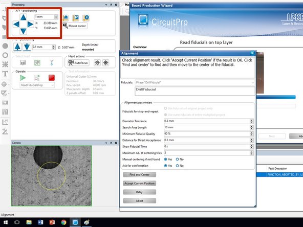
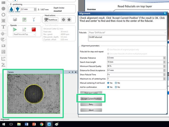
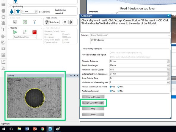
When the search stops you will be presented with the Alignment screen shown here. You should also see a yellow circle in the Camera output window. The circle's diameter matches the 1.5mm holes used for fiducial alignment.
-
The idea is to move the camera head using the X/Y positioning arrow buttons until you locate the 1.5mm fiducial hole you are looking for. You may need to change the motion increment.
-
Sometimes it is helpful to watch inside the mill as you are moving the head to gauge which direction and how far to move.
-
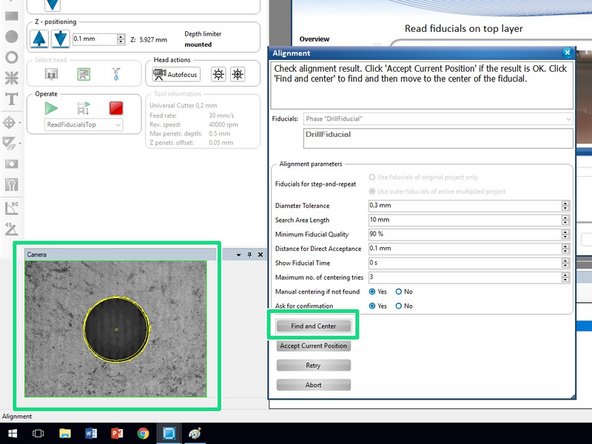
Once the fiducial hole is close to the yellow circle (it does not have to be in the center), click Find and Center within the Alignment window. The mill should automatically center over this hole.
-
Do not proceed if you cannot locate and center the fiducial holes as shown in this image, otherwise your mill job will fail.
-
-
-
It can be helpful to temporarily lift the mill lid and use a fine probe (the tip of a pencil works well) to point at the fiducial you are trying to locate on your PCB. You should confirm you see this reflected in the camera display.
-
If the camera displays your pointer, you may proceed. If you do not see your probe on the screen the camera is looking at the wrong 1.5mm hole. Note that the diameter of the fiducial holes is the same as those used for copper rivets!
-
Be sure to remove your pointing device and close the mill lid after confirming you have located the correct fiducial hole.
-
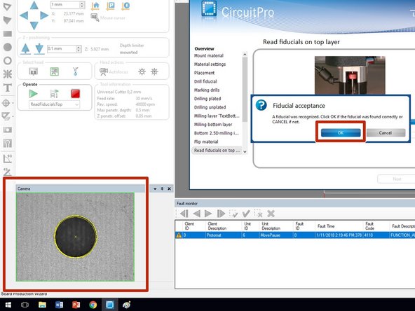
With the first hole successfully centered, click the Accept current position button.
-
The mill will now move in a counterclockwise motion to locate the remaining fiducials. Typically, it will find the next hole without issue. If it does not, you may need to again manually control the camera head to bring the fiducial into the camera display.
-
-
-
If the fiducial is detected automatically, click OK in the Fiducial acceptance window. Otherwise, click Accept Current Position in the Alignment window if you needed to manually assist in the location of the fiducial, following the procedure outlined in the previous steps.
-
Continue this process for the remaining fiducials. After all of the fiducials have been recognized and their positions have been accepted, the mill will continue by milling the top copper layer of the PCB.
-
-
-
After completing the top milling phase the mill will pause to again find the fiducial holes. While this step is not necessary from a production standpoint, it allows the user time to inspect the top layer prior to routing out the PCB.
-
The mill will stop moving and CircuitPro will display a Confirmation of focus height window. When you see this window, lift the mill lid. The bit will stop spinning and CircuitPro will temporarily display a window asking you to close the lid.
-
Being careful not to touch or move the copper clad, inspect the top layer of your PCB. Similar to when you inspected the bottom layer in a previous step, look to make sure that all isolation channels are free of debris, holes are aligned in the center of pads, etc. Refer to the list in the previous step.
-
It will be slightly more difficult to inspect your PCB this time as the milling head will be in the way for fiducial recogniation. Do the best you can.
-
If you believe your top layer may have some problems, please stop and alert a technician. If you stop now and ask for help you may be able to save your PCB, Maker-E resources, and a lot of time in the future.
-
If you feel your top layer is milled properly, close the PCB mill lid and continue with the tutorial.
-
-
-
If your top layer is good, and you have closed the mill lid, click Yes in the Confirmation of focus height window.
-
You will now need to repeat the procedure you followed previously when searching for fiducials after flipping the copper clad.
-
It may be necessary to manually move the head in small increments this time, which may not have been necessary during the first round of fiducial alignment. This is due additional debris generation during the top milling phase.
-
After confirming all of the fiducial holes the mill will drill three holes (one at each corner of your PCB) and then route out the space between these holes.
-
Be aware that the routing will take two passes. The first pass cuts our your PCB, the second pass cleans debris out of the routing channels.
-
-
-
When the mill finishes routing out your PCB, it will move the head out of the way and stop.
-
When the mill stops moving and you see the screen shown here, you may lift the lid of the mill.
-
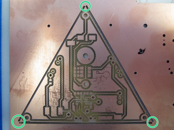
Again, inspect your PCB to ensure it milled properly. There is still time to correct any issues if they are present. See a Maker-E tech for help. Note that the PCB will be attached by three small tabs, one at each corner.
-
If your PCB looks good, remove the copper clad from the bed. Working your way around the three corneres, use gentle pressure to break the PCB free from the copper clad material.
-
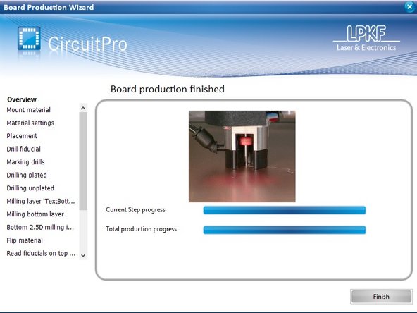
Close the mill lid and click Finish when you are done.
-
-
-
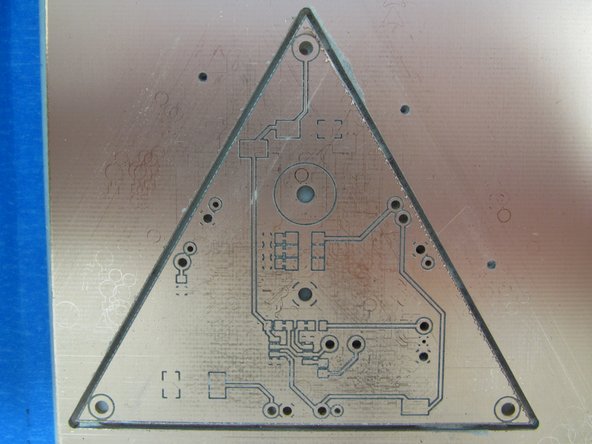
Similar to checking the bottom layer of your PCB, inspect your board to again confirm these points:
-
Isolation paths (areas where copper was removed) should appear sharp, clean, and consistent. There should be no burrs, breaks in the path, or missing paths.
-
Drill holes should be nearly perfectly aligned within copper pads. Holes should pass completely through the copper clad material.
-
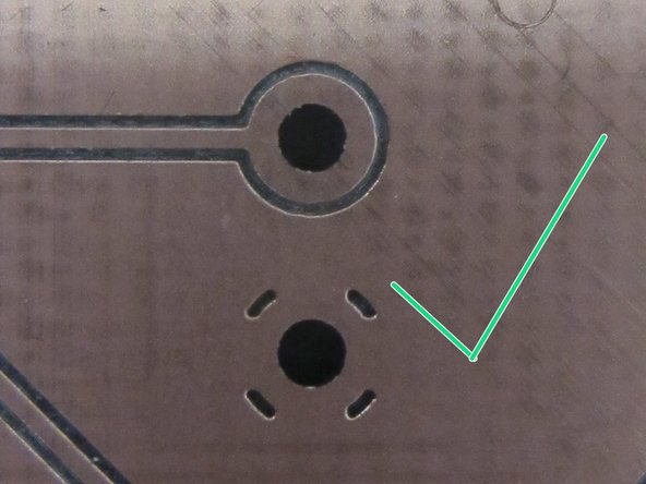
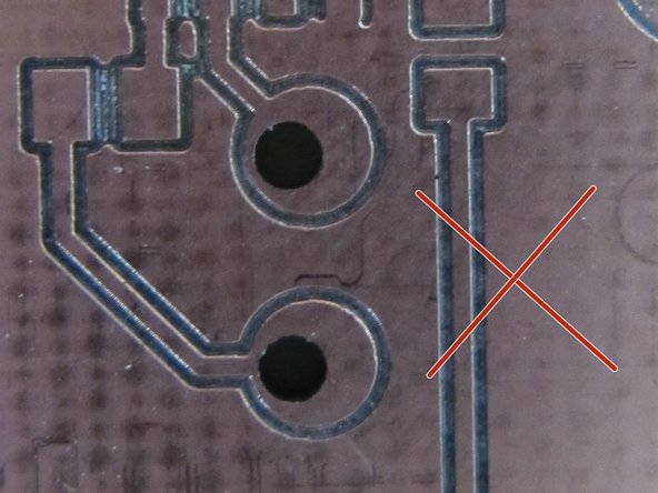
See the examples here for good and bad hole alignment.
-
Confirm that the alignment between holes and pads on both top and bottom layers is good. A small amount of offset is acceptable. Too much offset may cause issues with electrical shorts when you go to install copper rivets for vias and through holes. In this case you may need to mill a new PCB.
-
-
-
In order to avoid causing problems for the next user, it is imperative that these instructions are followed in the order shown here. Failure to follow the steps in this order will cause problems the next time the mill is used.
-
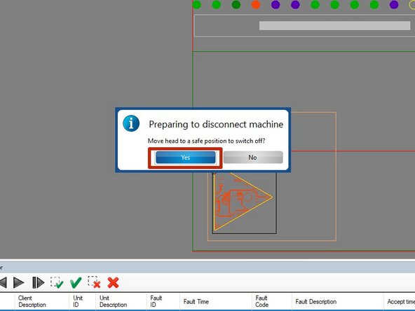
When your are done inspecting your PCB you can should down the mill. Select File -> Exit from the menu bar. When prompted, choose Yes to save your work.
-
When prompted to move the mill head to a safe position, click Yes.
-
Wait until the mill has stopped moving and the CircuitPro application has completely closed. Then you may lift the mill lid and turn off power.
-
Remove the PCB mill training card from the badging box and return it to a Maker-E technician.
-
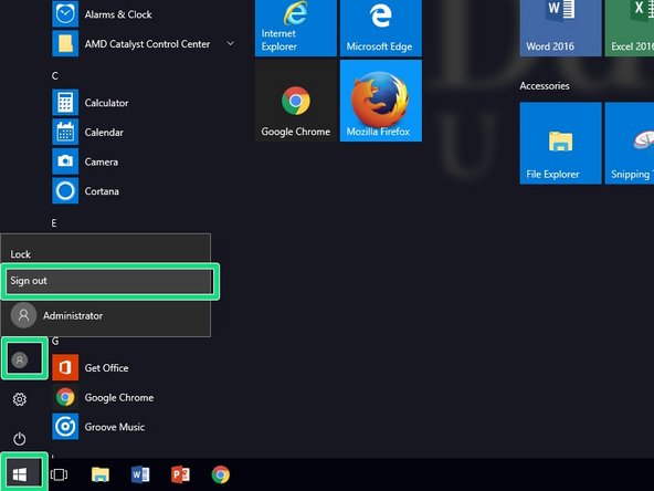
Finally, log out of the mill computer.
-
Remember to log out of the tablet as well!
-
-
-
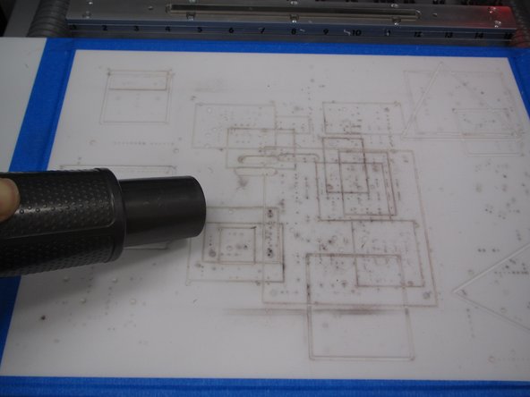
The oil from your hands will tarnish the copper. This corrosion will make it difficult to solder in future steps. You should pause to clean your PCB.
-
Locate a piece of 0000 gauge steel wool in the drawer below the PCB mill.
-
Move to a Maker-E bench that has a vinyl mat (such as the soldering bench), or place a piece of paper on top of a bare work surface to prevent scratching it.
-
Press the steel wool against your PCB and, using circular motions, buff both surfaces of your PCB to remove any corrosion or other debris. Try to avoid touching the surfaces of the PCB with your bare hands.
-
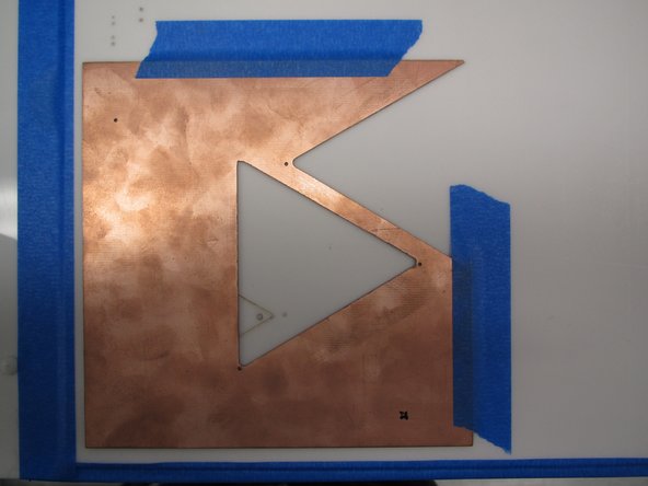
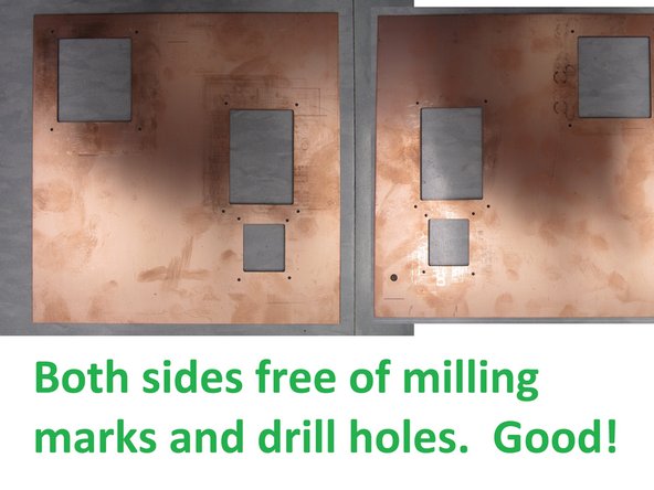
When finished, both sides of your PCB should appear clean and shiny like the example shown here.
-
Remember to clean up any mess you make when you are done. The steel wool will leave behind lots of little fibers.
-
-
-
If your PCB design contains plated through holes or vias you will need to use the rivet press to create conductive pathways in these holes to link the top layer to bottom layer. Check out the rivet press tutorial here.
-
Once you have your rivets installed you can move on to using the Pick and Place to place any surface mount components your PCB contains. When you are done placing and reflowing your surface mount components you may read the soldering tutorial to attach your remaining through hole components.
-


Cancel: I did not complete this guide.
9 other people completed this guide.