
Introduction
The placement of surface mount (SMT) components on a PCB is a much different process than that used for through hole components. The solder used for SMT is in a paste form and heat is applied to the entire PCB at once via a reflow oven, as opposed to individual components with an iron as used for through hole components. As SMT components are often very small and require precise placement and rotation it is useful to have a machine assist with the placement process. While it is possible to assemble SMT components on a PCB with the use of tweezers, wire solder, and a steady hand, we encourage all users of the Maker-E to use the pick and place for SMT components in order to decrease the chance of soldering errors.
Published by Ryder R. Nance with contributions from Matt P. Lamparter.
Tools
No tools specified.
Parts
-
-
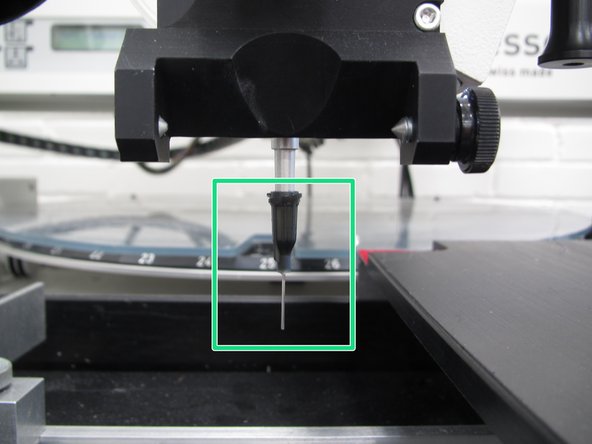
The Essemtec Expert SAFP is a semi-automatic pick and place machine. This devices allows the user to pick up small SMT components with a vacuum nozzle, use an optical microscope camera to aid in positioning, lock movement axes and dial in micrometer adjustments, and precisely place SMT components on a PCB.
-
The pick and place (PnP) will also dispense solder paste.
-
The PnP is a precision machine and as such is expensive. You should operate it with care. If you are using the machine and something is not operating properly or moving fluidly you should stop and contact the Lab Director. Excessive force can damage the PnP.
-
The placement head is the most delicate part of the PnP. It can move in the x and y directions within the plane parallel to the parts carousel.
-
When moving the placement head you will have to be aware of obstacles such as the parts carousel, the PCB, and the handrest. It is easy to bump the head into these obstacles, so it is important to follow the path of motion as you are moving the placement head to avoid any possible collisions.
-
-
-
The solder paste used in the Maker-E contains lead. As long as you follow the guidelines in this tutorial you will not be exposed to lead. However, failure to follow these guidelines could expose the user to a small amount of lead.
-
Users should wear gloves while handling the solder paste and working with the pick and place.
-
Nitrile gloves can be found in the yellow DeWalt cabinet in the Fabrication area of the Maker-E.
-
-
-
Do not eat or drink (this is not allowed in the Fabrication area of the Maker-E, as outlined in the Maker-E User Agreement you signed).
-
Do not touch the paste with your hands. If you need to remove or clean up paste, use a paper towel.
-
Use caution when handling paste tubes with fine nozzle tips. These tips can pierce skin if enough pressure is applied.
-
Avoid touching your hair and face.
-
Wash your hands when you are done handling solder paste.
-
-
-
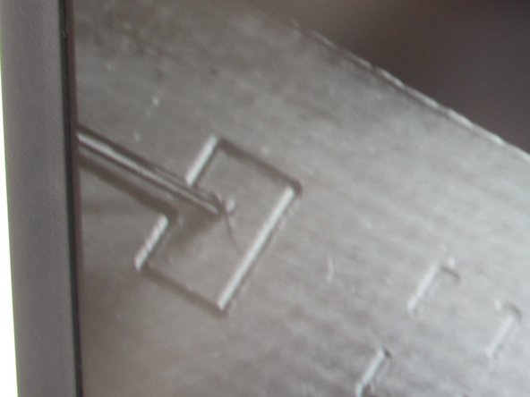
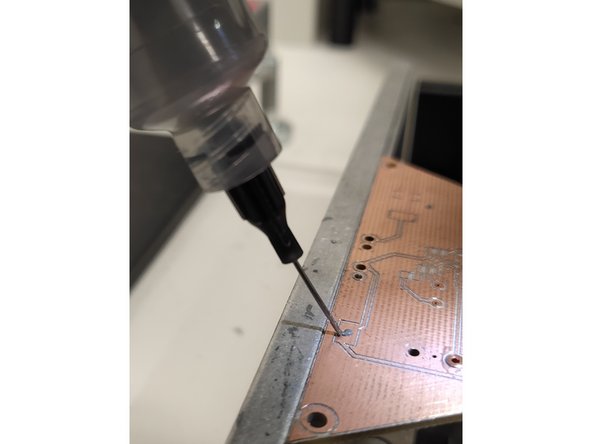
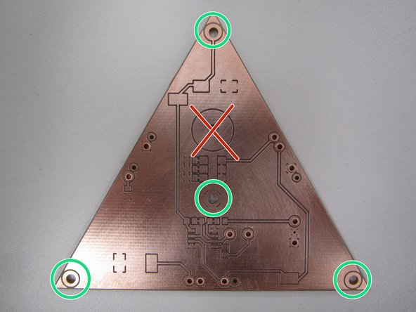
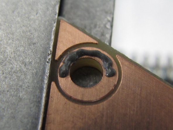
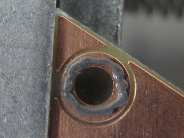
Note: if your PCB was milled using the PCB mill in the Maker-E, and it contains vias or plated through holes, be sure to install the copper rivets before placing SMT components.
-
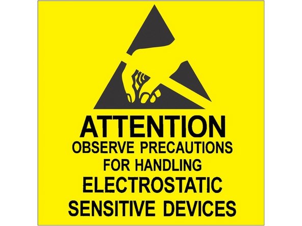
Before proceeding, you should be familiar with electrostatic discharge (ESD).
-
Two common examples of ESD (Not to be confused with ESP) events are lightning, and the shock you may have experienced on a winter day when touching something metal after walking on tile or carpet. While harmless to humans, this rapid dissipation of stored electric charge can cause serious damage to sensitive electronic components.
-
The LMC555 timer used in the firefly is one such device. Check out page 4 of the datasheet for ESD information.
-
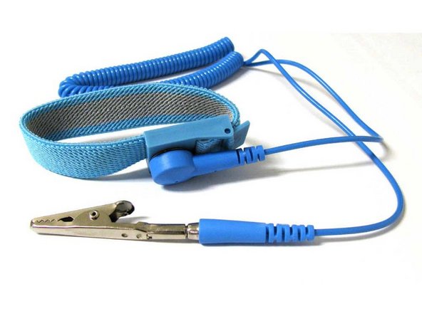
It is best practice to always wear a properly grounded static strap when handling your components. These straps allow any excess charge which has accumulated on your body to slowly and safely dissipate to ground. Straps are available at nearly all of the benches in the Maker-E.
-
-
-
Locate the static strap to the left of the PnP. It usually falls to the left of the bench.
-
Slide the strap around your left wrist and make sure that the metallic part of the strap makes contact with the skin of the inner part of your wrist.
-
To function properly, the strap MUST make full continuous contact directly with the skin on your wrist. Do not use the strap on top of clothing.
-
The wrist strap has a connection point which is detachable via a snap. This allows the user to move away from the bench temporarily without having to remove the wrist strap.
-
Be sure to reconnect it when you return as you most likely have accumulated a small amount of charge while moving away from the bench.
-
-
-
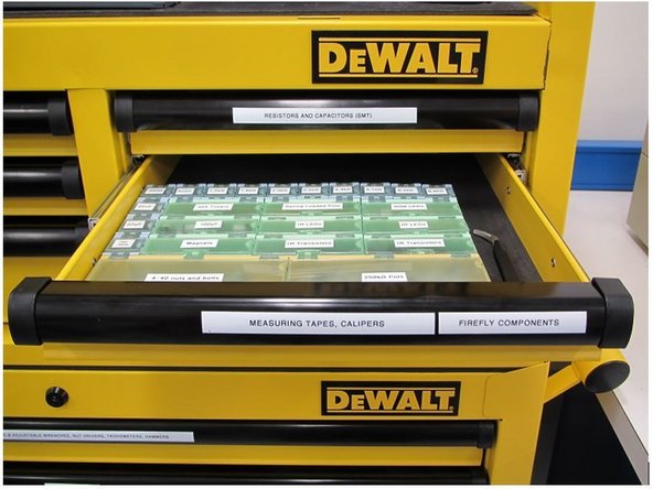
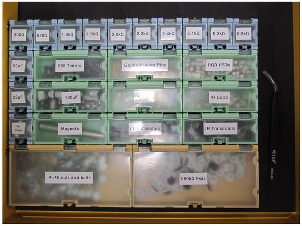
Make sure you have all of your SMT components on hand before you begin to place solder paste. If you are populating a firefly board you can find the container with all of the components in the yellow DeWalt cabinet. Look for the drawer on the top right labelled Measuring tapes, calipers and Firefly components.
-
The component bins are all labelled. It is recommended to take this entire container over with you to the pick and place machine. There is a set of tweezers in the drawer to aid in picking components out of the bins. Please be sure to return these tweezers to the drawer, along with the components, when you are finished.
-
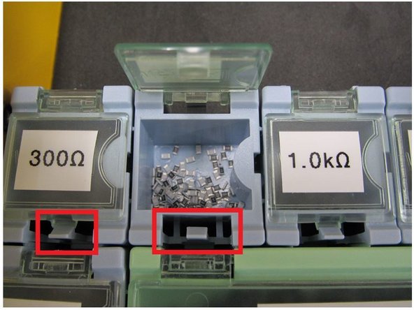
The lid to each bin is spring loaded. Gently pull back on the clip of each bin to open the corresponding lid.
-
Surface mount resistors and capacitors are extremely small. Only open one bin at a time to avoid mixing up components. The 0805 capacitors have no marking on their package, so it is impossible to identify them once they are out of their labelled bin.
-
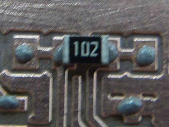
The resistors have values marked on them using a code similar to the resistor color code used on through hole resistors.
-
The code is read from left to right. For resistors with three digits the first two digits are significant figures and the third is a multiplier. For resistors with four digits the first three are significant figures and the fourth is a multiplier. The multiplier is a power of 10.
-
For examples of how to read this code, see the Packages page
-
-
-
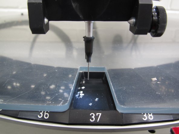
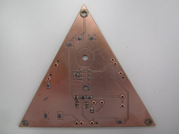
Install your PCB in the board cradle. The left edge of the cradle is spring loaded. Apply a small amount of pressure to your board as you push it to the left.
-
Now slide the right edge of the holder over to the meet the right edge of your PCB. You may need to loosen the thumbwheel to move the holder. Once your PCB feels secure, tighten the thumbwheel.
-
Your PCB should now be securely held in the cradle. Try to gently push on the board to make sure it is secure. If the board can move, repeat the previous few steps in order to achieve a more secure hold in the cradle. You should also slide the hand rest over to the right edge of your PCB.
-
-
-
Your first task is to dispense solder paste onto your board. Solder paste is typically found in two different types of containers. A large tub for application via a stencil, or in small tubes for application via compressed air. The PnP will use the compressed air method to dispense small amounts of paste on all of the conductive pads on a PCB.
-
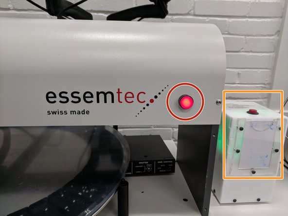
Insert your makerspace badge into the badging box. If you are not yet certified, obtain a training card from a technician.
-
Begin by turning on the PnP with the red power button on the right.
-
When you power up the machine, compressed air will be sent to the head. This makes a popping sound and sometimes the paste dispenser tubing will fly up.
-
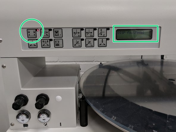
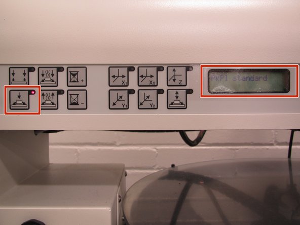
By default the machine starts in placement mode. You should switch to paste dispense mode. Press the Paste dispense button on the far left. A red light should illuminate immediately to the right of the button and the LCD should display “DISP footPedal.”
-
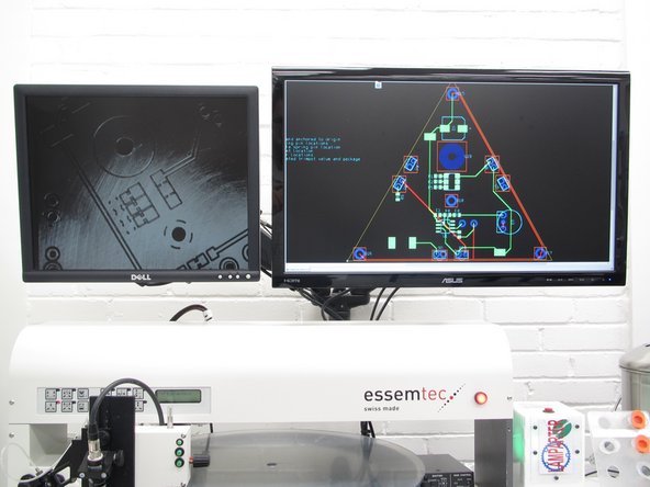
Turn on the left LCD monitor to view the microscope camera. The right monitor can be used with the computer to view your PCB design files. It is recommended that you open your PCB design file in Ultiboard so you can distinguish PCB pads, traces, etc. and properly identify components.
-
-
-
Solder paste has a shelf life between six months and one year. The shelf life is prolonged if the paste is kept refrigerated. However, in order to dispense paste properly and avoid reflow issues it is recommended to use solder paste at room temperature. As such, the solder paste in the Maker-E is kept out of refrigeration.
-
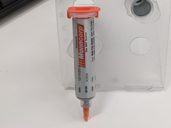
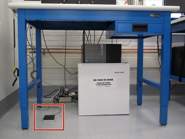
Locate the stand with the tubes of solder paste. Select a tube and remove it from the stand.
-
Remove the orange stopper from the opposite end if there is one.
-
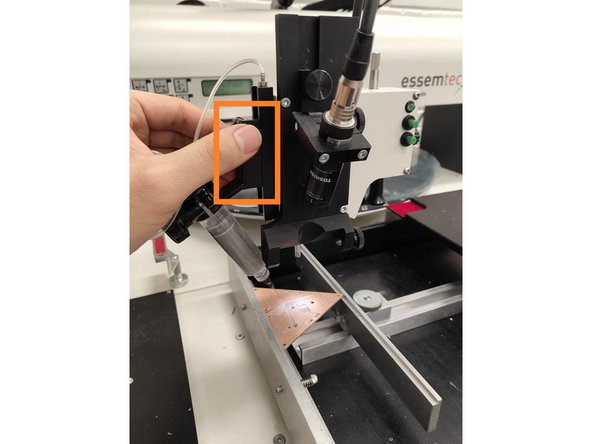
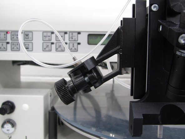
Locate the solder paste connector tube attached to the placement head.
-
Push the open end of the solder paste tube onto the tube connector. Align the connector collars so that they are perpendicular to the tube ends.
-
Rotate the tube connector 90° so that the collars grab the tube ends. If you don't do this, the tube will fly off of the connector.
-
-
-
Insert the solder paste tube into the tube holder on the left of the placement head. You should move the arm of the pick and place out towards you, and away from the parts carousel. This will prevent the solder paste tip from hitting the carousel.
-
If there is not already a BLACK dispensing tip on the solder paste you are using, you will need to put one on. You can move one from another tube, or get one from a technician. DO NOT use a tip from the drawer!! These are for placement only. Putting solder paste in these tips may clog the machine if they are sucked into the vacuum system.
-
The clear rubber tubing attached to the holder provides compressed air to the solder paste tube. Once compressed air is applied to the paste tube a small amount of paste will be dispensed from the black nozzle tip at the end of the paste tube.
-
-
-
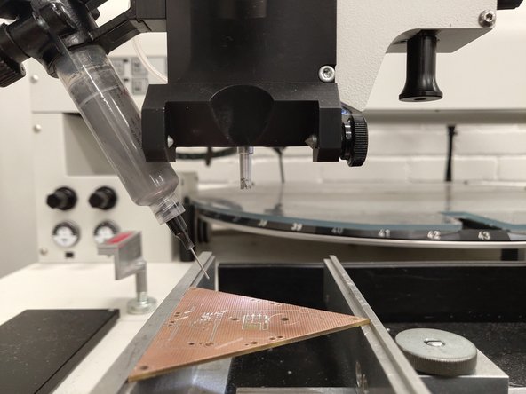
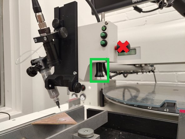
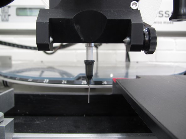
Hold the black placement knob on the lower right side of the placement head and slowly move the placement head so that the tube is over the top of your PCB. Make sure that there is clearance between the end of the solder paste nozzle and the PCB. You want about a half inch vertical gap between the end of the nozzle and the PCB.
-
Do not use the horizontal black knob. This knob controls the z-axis range of motion and should not be adjusted.
-
If you need to adjust the gap between nozzle tip and PCB, you can move the paste tube holder up and down within the channel where it attaches to the placement head. Use one hand to steady the placement head while you use the other hand to move the tube within the channel.
-
-
-
You should also confirm that the nozzle tip is visible in the microscope display. If you cannot see the tip it may be necessary to adjust the paste tube up or down.
-
Note that using the microscope display is optional. Some users prefer to watch the PCB, nozzle tip, etc. directly without the aid of the microscope display. It is personal preference and you should choose what you are most comfortable with.
-
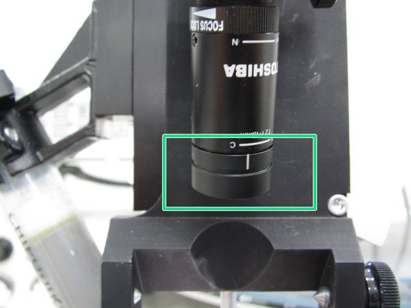
It may be necessary to adjust the aperture ring of the camera in order to allow more or less light into the image.
-
-
-
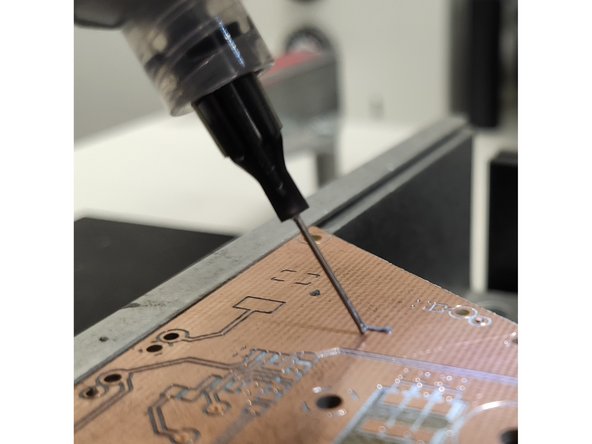
Now pull down on the black placement knob to slowly lower the tube. Watch the nozzle tip in the monitor or at the PCB itself. Confirm that the nozzle tip can just touch the surface of the PCB. Be careful not to extend the head too far down and bend the tip.
-
If you cannot touch the surface of the PCB you will need to adjust the paste tube up or down.
-
-
-
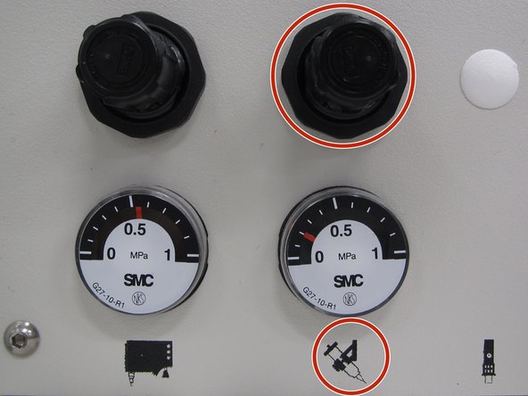
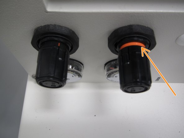
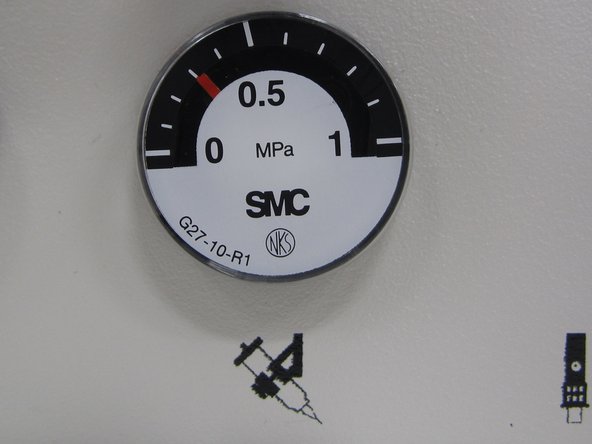
It is important to adjust the pressure used to dispense solder paste. Find the pressure adjustment knob at the left side of the PnP. Be sure to locate the paste dispensing pressure knob, not the head pressure knob.
-
Pull out on the knob until the orange ring is exposed. Rotate the knob clockwise to increase paste dispense rate (pressure) or counterclockwise to decrease dispense rate. A good starting point is 0.3 MPa.
-
When you have the correct pressure, push the knob back in to lock in the pressure setting. The orange ring should no longer be exposed when you are finished setting the pressure.
-
As you gain familiarity with the dispensing process and feel comfortable, feel free to increase the pressure to dispense paste faster.
-
-
-
You are now ready to dispense paste. Locate the foot pedal below the PnP. You may need to pull it out from under the bench so that it is easily accessible. You should be standing in order to use the foot pedal while dispensing paste.
-
If this is your first time using the PnP you should begin in an empty section of your PCB where there are no traces or pads. This will be your practice area. Using the black knob, pull the nozzle down until it just meets your PCB.
-
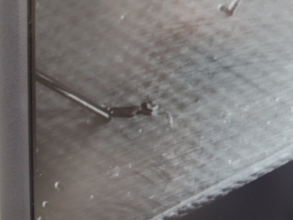
Hold down the foot pedal to engage the pressure to the paste tube. You should see a small amount of paste dispensed from the nozzle. To avoid a large blob, slowly move the nozzle from right to left with the placement knob while holding down the foot pedal.
-
Once you release the foot pedal the pressure will be removed from the paste tube and paste dispensing will stop. Drag the nozzle a millimeter or so to the left to remove excess paste from the tip and then allow the tip to rise from the PCB.
-
Spend a brief period of time familiarizing yourself with the paste dispense process. Your application will improve with practice. You can adjust the pressure dial up or down as you are comfortable. Do not exceed 0.6 MPa.
-
When you are done experimenting you may leave the paste on the PCB or use a small piece of paper towel to remove it. If you choose to remove the paste, be careful not to smear it into any surrounding isolation channel, traces, or SMT pads. This could cause bridging during reflow.
-
-
-
Here are some guidelines when dispensing solder paste:
-
When dispensing paste on a pad, always move the dispensing tip from right to left. This will prevent an excess of paste from building up on the nozzle tip.
-
Always release the paste pressure (foot pedal) slightly before you wish paste dispensing to stop. Then drag the tip over the last portion of the pad to remove paste from the nozzle tip before bringing the tip up from the PCB.
-
When applying solder paste, begin on the right side of your PCB. Apply paste to the right-most pads, and then move to the left side of the PCB.
-
If an excess or blob of paste accumulates on the nozzle you can remove it using a small bit of paper towel.
-
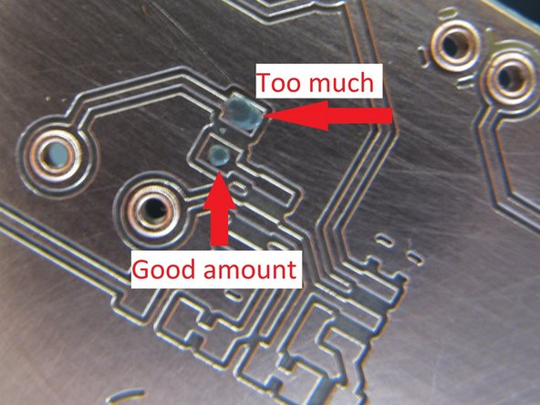
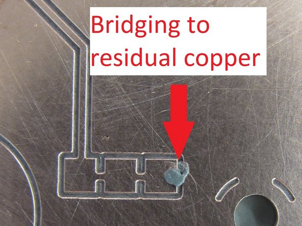
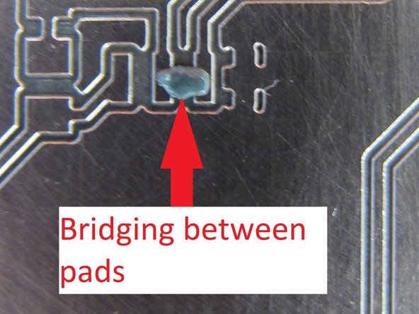
In general, the rule of “less is more” applies when dispensing solder paste. It is very easy (particularly with copper clad boards created on the PCB mill) to apply too much paste and cause bridging between pads or onto residual copper. It is not necessary to completely fill a SMT pad with paste but rather cover perhaps 50% of the surface area.
-
-
-
Now go through and dispense solder paste on all of your SMT component pads. Consult your PCB design file in Ultiboard using the right monitor. Make sure to dispense paste on all of your pads.
-
If you encounter a large pad, it may be necessary to hold down the pedal longer to dispense a larger amount of paste. Try to keep the paste from forming a blob on the tip. Be sure to continue to the move the tip around the pad while dispensing paste in a serpentine fashion.
-
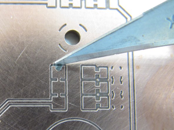
If you feel you have dispensed too much paste, or you have bridged paste between pads or onto the residual copper, it may be necessary to remove paste. You can use a small bit of paper towel to do this, or a fine knife blade.
-
-
-
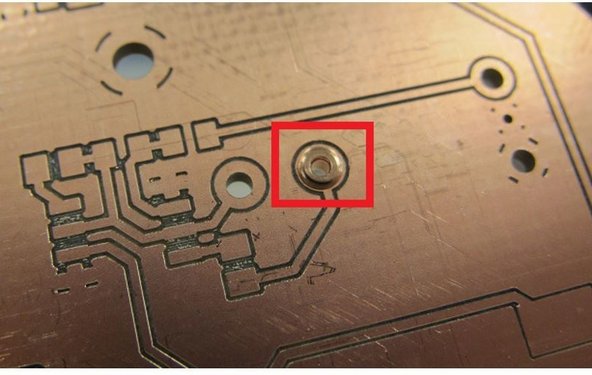
If you are applying solder paste to a PCB created using the PCB mill in the Maker-E you will need to add solder paste to the rings around the holes for the four spring loaded pins that bring power and ground into your circuit.
-
Do not apply paste to the large ring slightly above the center of the board. This ring is for the magnet and does not require solder.
-
These pins are not SMT components but adding paste to these rings will aid in the through hole soldering process later.
-
Do not do this for any other through hole components, just the rings for the spring loaded pins.
-
In order to apply paste to these rings, start at the right edge of the ring (3 o’clock) and move around the top half of the circle (to 9 o’clock). Then release the foot pedal, reset the nozzle to the right edge again (3 o’clock) and dispense paste around the bottom half of the circle.
-
This will minimize dragging the tip through the paste and accumulating paste on the tip, or creating unwanted bridging. Do not forget the hole in the center of the PCB, in addition the the holes at each of the three corners.
-
-
-
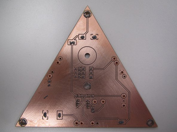
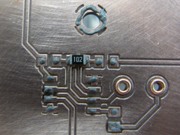
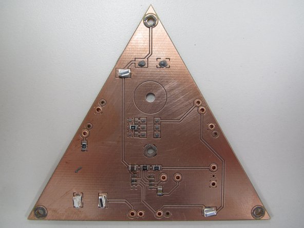
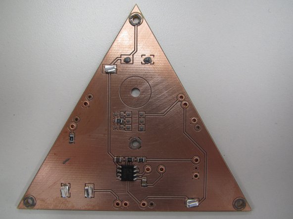
When you have paste applied to all of your SMT pads, as well as the spring pin rings, your board should look similar to this example.
-
When you are done dispensing paste, use the placement knob to move the nozzle away from your PCB. Pull the paste tube out of the holder. Rotate the tube connector 90° so that the collars are perpendicular to the tube wings. Rock the tube connector back and forth as you pull upwards in order to remove the connector from the tube.
-
Replace the orange cap on the solder paste tube and return the tube to the stand to the right of the pick and place.
-
Leave the tube connector resting in the holder for the solder paste tube.
-
-
-
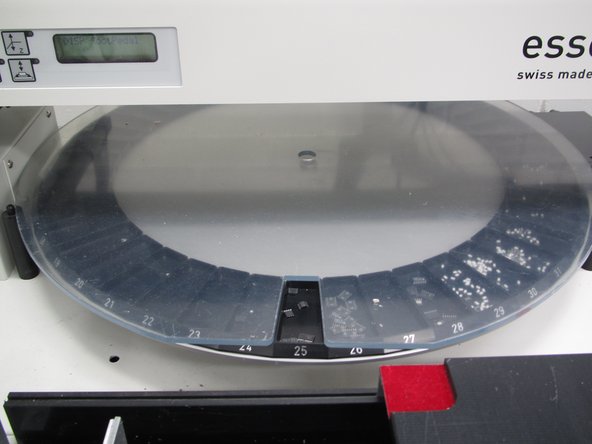
You are now ready to begin placing components. Begin by placing your components in one or more bins of the 45 bin carousel tray.
-
Return the PnP to placement mode. Push the Placement mode button on the left panel of the PnP. The corresponding red light will illuminate the LCD will display “PkPl standard.”
-
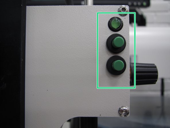
You can rotate the carousel by using the two green buttons on the placement head. You may group the components together in a single bin or place one component per bin. Just remember which component is assigned to each bin. It may necessary to occasionally adjust the clear plastic lid on top of the tray to align the opening with the bins.
-
-
-
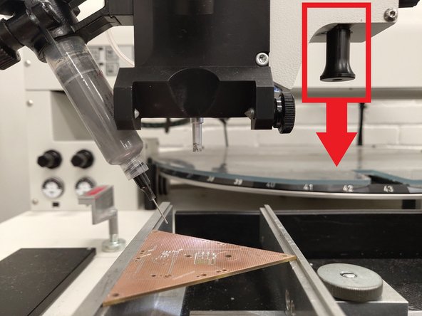
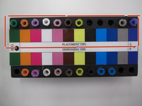
Open the drawer below the PnP and locate the nozzle tips. Choosing from the side labelled PLACEMENT TIPS, select a tip size that will allow you to pick up the majority of your components.
-
Vacuum will be applied to this tip, so be sure that the tip can entirely fit on top of the components you wish to pick up with it. Be careful not to select a size too large, as it is possible for small components (resistors, capacitors, etc.) to fit inside of the larger tips and be sucked up by the vacuum.
-
If you are working on the firefly PCB, the black tip is a good size.
-
Remove the tip from the holder and gently push it onto the nozzle end of the placement head. It is helpful to push the tip on with one hand and keep the placement head steady with the other hand applying pressure from the top.
-
If the vacuum engages (placement head light turns green and you hear a vacuum noise), simply grab the black plastic of the nozzle tip and push up gently while pulling down on the placement knob to disengage the vacuum.
-
-
-
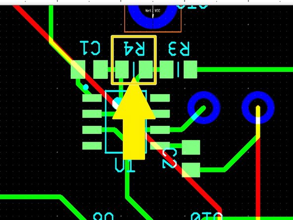
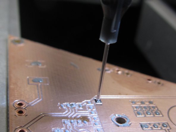
Examine your PCB layout file in the computer monitor. Choose which component you will place first and locate it on the PCB layout. Be sure to check the reference designator, part number, or value to match this with the physical component you are about to place.
-
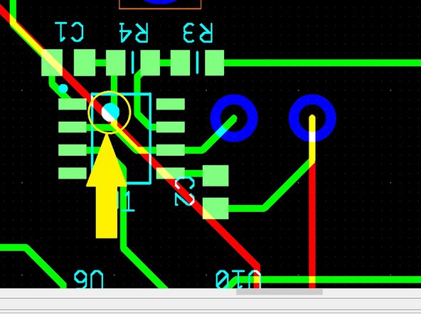
In the example shown, the component to be placed is resistor R4.
-
-
-
Using the green buttons on the placement head, rotate the carousel to open the bin containing the first component you wish to place. Here are some guidelines when choosing which order to place components:
-
Work from the inside of the PCB to the outside. You are less likely to bump into previously placed components this way.
-
Start with small components (resistors, capacitors, diodes, etc.) and then move onto larger components. This will aid in visual placement, as often larger components will obscure smaller components.
-
Leadless packages such as QFN and BGA are very difficult to place, particularly on copper clad boards without silkscreen. These packages should be avoided in your design if at all possible.
-
-
-
Use the placement knob to move the tip over the center of the first component you want to place. Pull down on the placement knob until the tip just touches the center of your first component, in this case a resistor.
-
Note that resistors contain a label indicating their value. The code is typically three or four digits in length. The first two or three digits indicate significant figures while the last digit is a multiplier. For example, 682 would be a 6.8 kΩ resistor: 68 * 102.
-
If the nozzle will not extend far enough to pick up a component, or the vacuum will not engage, please see the Lab Director for help.
-
When the tip makes contact with the component, continue to gently pull down on the black knob. The vacuum will engage, as indicated by a click sound followed by a continuous hiss. The green light on the placement head will illuminate.
-
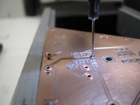
Slowly raise the placement knob. As the nozzle tip rises the component should be carried with it, held in place by vacuum.
-
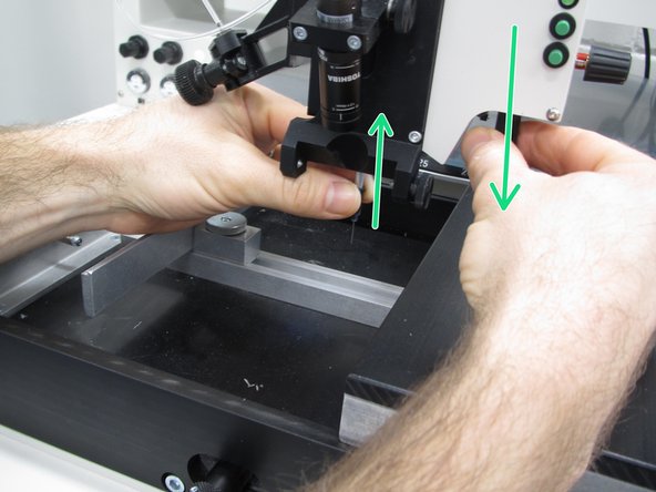
Now carefully move the placement head so that the resistor is over top of the PCB in the general area of the pads where it needs to be placed. When moving the tip be careful of obstacles like the handrest, carousel tray, and board cradle. Do not bump the nozzle tip against any obstacles or you could lose your part or damage the tip.
-
-
-
Viewing the PCB directly, or watching the microscope display, align the component over the appropriate pads on the PCB. Rotating the black placement knob will rotate the component.
-
Slowly pull down on the knob to better align the component. When you are confident the component is properly aligned, pull the knob down all the way to place the component on the pad containing solder paste. Apply enough downward pressure to disengage the vacuum (green light should go out and hissing should stop).
-
After the vacuum disengages, the component should be held in place by the solder paste while the nozzle tip travels back up.
-
It is best practice to use consistent rotation and orientation when placing resistors and capacitors. For example, you may wish to orient all of your horizontal resistors right side up for ease of reading the values. Similarly, keep 90 degree rotations all the same direction to aid in reading of values during troubleshooting.
-
-
-
Congratulations, you just placed your first SMT component! Here are a few points worth mentioning:
-
The reflow process will “pull” the components into placement slightly. If a component is not 100% in alignment this will be corrected somewhat during reflow in the oven.
-
However, it is still important to align the component with the pads as best you are able in order to avoid solder bridging. This is particularly important for PCBs created on the PCB mill in the Maker-E.
-
Try to avoid removing components after they have been placed. If you must remove a component, use a pair of tweezers. Examine the SMT pads to determine whether or not you need to re-apply solder paste.
-
-
-
Rotate the carousel if necessary and locate the next component you wish to place. Continue the process described above to place all of your 0805 resistors and capacitors. Some notes on the capacitors:
-
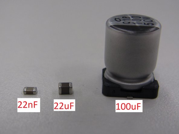
Two of the capacitors in the firefly circuit are in the 0805 package. Unfortunately, capacitors in this package lack the marking that resistors have so there is no way to tell them apart. BE SURE YOU KNOW WHICH VALUE CAPACITOR YOU ARE PLACING.
-
The 100 μF capacitor is in the “aluminum can” package. This is a larger package and should be placed near the end of the placement operation. Instructions for placing this component are provided in a following step.
-
-
-
Place the test points next. Continue to check the PCB layout on the computer monitor to ensure you are placing components in the proper location.
-
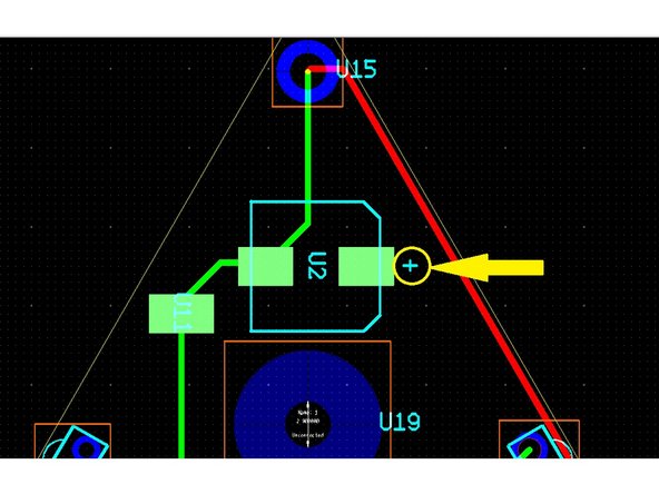
Be careful with the test points, it is easy to mistake the pads for the 100 μF capacitor as pads for two test points.
-
-
-
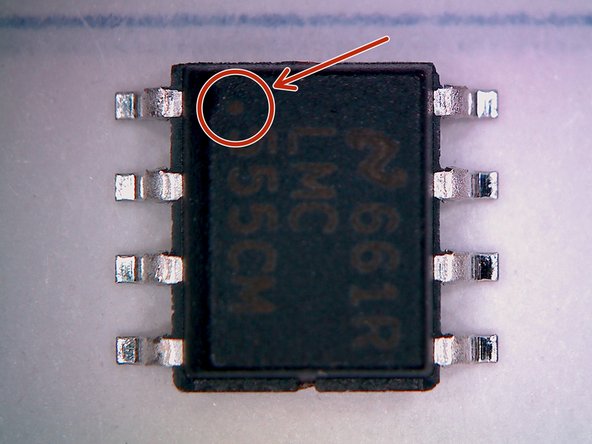
Now place the 555 timer. This component is housed in an 8-lead SOIC package. As this package is symmetric it is important to note the correct orientation. This is often accomplished via a small dot on the package, indicating pin 1.
-
Check your PCB design file to make sure you align the 555 timer properly.
-
-
-
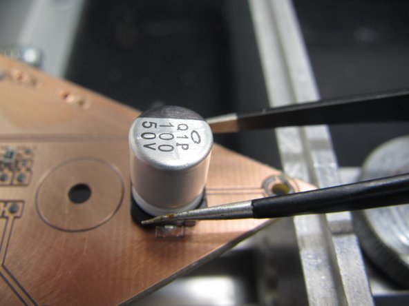
Next, place the 100 μF capacitor in the can package. Since this is an electrolytic capacitor, polarity matters. Refer to your PCB design file for proper orientation.
-
Note that this capacitor package is so tall, and the footprint relatively large, that it may be easier to place by hand with a pair of tweezers instead of using the pick and place.
-
-
-
Finally, place the RGB LED. This package is also symmetric and has an indicator to aid in proper alignment. Again, consult your PCB design file to properly orient the LED.
-
This package does not have any leads that stick out, which makes placement slightly more difficult. When placing the component, bring it down so that it is almost touching the paste. Then view the PCB directly (as opposed to the microscope display) to aid in proper placement.
-
Look at both sides of the LED package to ensure that the leads under the package align with the PCB pads.
-
-
-
After you have placed all of your components, move the handrest to the right and carefully loosen the thumbscrew securing your PCB in place. Gently lift your PCB out of the cradle.
-
While the paste is sticky enough to hold the components in place, it is not glue. Use caution when moving your PCB so as not to disturb component placement.
-
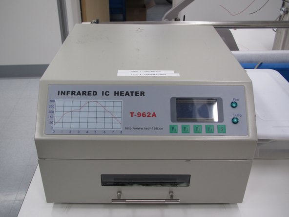
In order to finish the placement process you must reflow the solder paste. This means your board will be placed in an oven and gradually heated. During this process the sticky part of the paste will boil off and remove impurities from the component pads.
-
Next the solder will melt and finally the board will cool rapidly to form good mechanical and electrical connections.
-
-
-
Before moving onto the reflow oven, be sure to remove the placement tip from the pick and place and return it to the proper location in the drawer.
-
Remember to turn off the pick and place and return the training card to a Maker-E tech. Turn off the video monitor as well and log out of the computer.
-
Also be sure to clean up any scraps of plastic, paper towel, etc. and leave the area clean. Solder paste should be cleaned up as well.
-
-
-
The final step is to reflow the solder paste on your PCB. This will melt all of the solder at once and securely adhere your SMT components to the PCB.
-
Please see the reflow oven tutorial to continue.
-


Cancel: I did not complete this guide.
34 other people completed this guide.