
Introduction
For this tutorial we will use NI Multisim to lay out a circuit. We will focus on designing and connecting the circuit and leave simulation to the user to explore on their own.
The specific circuit we will be designing is an electronic firefly, inspired by a 1993 article in Scientific American. In nature, individual fireflies blink their light at a certain frequency, independent of other fireflies. When one firefly encounters another, their lights begin to synchronize and flash in unison. Our circuit mimics this behavior. A light will flash with a rate that can be modified by the user. When the circuit aligns properly with another firefly circuit, the two will cease to flash independently and begin to flash in unison.
| More Information | |
|---|---|
| There is a lot of existing documentation on using Multisim and Ultiboard. Please begin by reading these tutorials provided by NI. This will allow you to familiarize yourself with the software interface and the basic features. | ● Introduction to Multisim/Ultoboard(up through part 4) ● Creating a Custom Component in Multisim ● Using on-page and global connectors in Multisim (up through part 5) |
| Prior to using Multisim and Ultiboard for the first time, please follow the link at the right to gain an understanding of how the component database system works and how to make some modifications to this system to facilitate easier component management, reuse, and sharing. | Moving a User Database to the network |
| Once you have a basic understanding of how to use Multisim, download and open the firefly circuit. The circuit you will be working with is missing a few components which you will have to add or create and connect properly. | Firefly Multisim File |
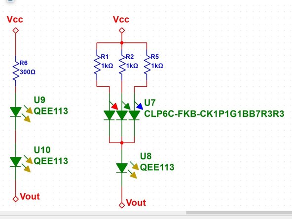
| You can view an image of what your final, completed circuit should look like by following the link on the right. Pay attention to the “reference designators” or RefDes of the IR diodes, U9 and U10. Make sure that your refdes values match what is shown in the completed circuit. More on this later. | Completed Circuit |
Published by Ryder R. Nance with contributions from Matt P. Lamparter and Daniel T. Vasquez.
Tools
No tools specified.
Parts
-
-
Begin by launching Multisim and opening the partial firefly schematic (.ms14 file) linked to at the top of this tutorial.
-
Your first task is to connect the emitters of the three IR photo transistors (QSE113) to the power source. The power source is represented by an on-page connector labelled Vcc. Place an on-page connector labelled Vcc and then connect it to all three transistors as shown in the example here.
-
Do not copy and paste on-page connectors. Doing so will cause their names to change and the virtual connection will be broken.
-
-
-
Next, you need to place a 22nF capacitor in your schematic and connect it between the CON pin of the LMC555CM timer and ground as shown in this example. Capacitors can be found in the Master database. A ground connection can be found in the Master database as well, or you may copy and paste an existing ground connection.
-
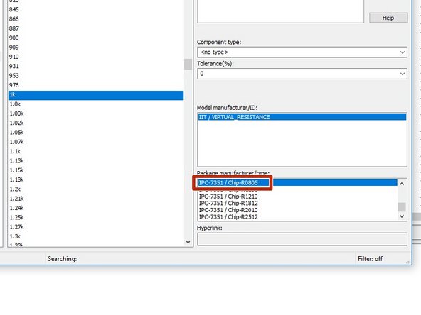
When choosing your capacitor, not only do you need to specify the value (22nF in this case) you also need to choose the correct package - the physical realization of your part. Image two here shows two 22nF capacitors. Both have the same capacitance value, but they are housed in different physical packages. More on this later.
-
Most of the resistors and capacitors used in this circuit will be in the 0805 package. When placing your 22nF capacitor, be sure to choose the Chip-C0805 package within the Select a Component window.
-
-
-
You will need to place two IR LEDs (QEE113) in series with a 300Ω resistor in Multisim. These components can be found in the Corporate database.
-
When placing the components, be sure that your reference designators (refdes) match what is shown in the example image: U9 and U10. If your refdes values are different there will be problems when you go to transfer your design to Ultiboard later in the tutorial.
-
This requirement arises due to the fact that the physical placement, location and orientation of certain components, including the IR diodes, is crucial to proper operation. As such the IR diodes have already been placed for you on the PCB (Ultiboard, not Multisim) with refdes values of U9 and U10.
-
If your IR LEDs in Multisim have refdes values other than U9 and U10, then transferring to Ultiboard will result in changes to diode placement.
-
-
-
Multisim ships with a master database of many components. However, the database is not exhaustive and may not contain all of the parts you need for your circuit. If you search the master database and your part is not found, you may need to create your own part.
-
If the part you are using is something that the Maker-E stocks, you can find it within the corporate database. The QEE113 IR LED is one such part. Be sure to specify the corporate database when placing this component.
-
-
-
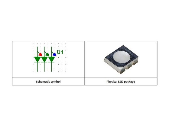
The final step to completing the firefly circuit is to place an RGB LED (red/green/blue light emitting diode) and the associated resistors. The values of the resistors determine the color of your light. You may choose which resistor values to place from the table in the next step.
-
Note that depending upon which color you desire for your light you may only place one or two resistors and leave the remaining space(s) empty.
-
The 1k resistor values in this example are purely for illustrative purposes. Your design should use values from the table in the next step.
-
-
-
Begin by placing the resistors. Suggested resistor values are shown in the table provided.
-
Similar to the capacitor you placed previously, when placing your resistors, not only do you need to choose the correct resistance value (from the table provided) but you also need to choose the correct package - 0805 in this case.
-
Note that a resistor with a value of "DO NOT PLACE" means that there is no connection on the corresponding pin of the RGB LED. This does not mean you directly connect the corresponding pin to VCC.
-
-
-
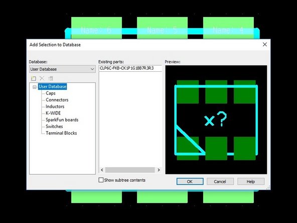
With your resistors placed, it is now time to place the RGB LED. The part number is CLP6C-FKB-CK1P1G1BB7R3R3.
-
This part is not in the master database. The Maker-E stocks this component, hence it can usually be found in the corporate database. However, during the instruction of course ECEG 301 this component has been removed.
-
For the purpose of this tutorial you are tasked with creating your own footprint and component in Ultiboard and Multisim, respectively.
-
We will begin by creating a custom footprint for the LED. Because footprints correspond to the physical realization of electronic components, you will need to use Ultiboard. Launch Ultiboard and follow this tutorial from NI to familiarize yourself with the process of creating a custom footprint.
-
You may skip the "3D Land Pattern" portion of the NI tutorial.
-
-
-
Once you feel comfortable with the component creation process it is time to create your LED component.
-
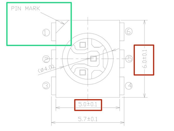
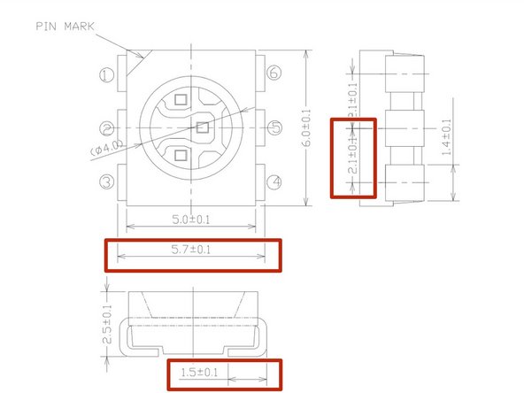
A link to the datasheet for the LED can be found here. Open the datasheet and examine page 7, highlighted here. Often datasheets will provide a defined footprint with dimensions of pads, pin pitch, etc. This datasheet does not go that far so it is up to you to infer these parameters from the measurements of the component itself.
-
-
-
Launch Ultiboard. Choose to create a new project of type PCB design. Launch the Part wizard in Ultiboard (Tools -> Part wizard) and choose to create a surface mount (SMT) part.
-
Click Next.
-
-
-
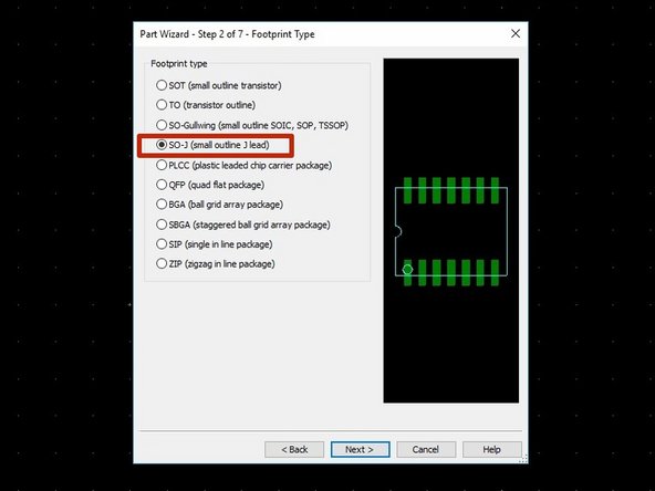
Our LED is in a package type called SOJ (small outline J-lead). Choose the appropriate footprint type in the next window. Don’t worry about the fact that the number and location of pins do not match our LED. We will correct this shortly.
-
Click Next.
-
-
-
Set your dimensional units to match what is given on your datasheet. In this case the measurements are metric, so choose mm.
-
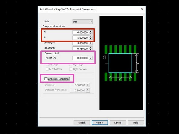
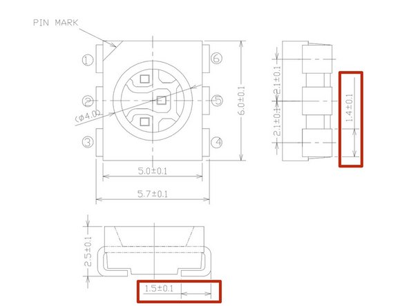
You need to specify the dimensions of the entire plastic component package. Examine the datasheet for this information. Note that there are tolerances (±) associated with many of the dimensions. For now we will ignore these.
-
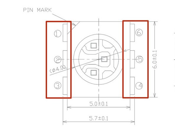
Many electronic component packages are symmetrical about one or two axes. This could cause ambiguity when placing components. In order to ensure proper orientation, there will often be a “pin 1” indicator, often realized by a notch in the chip or a small circle printed on the package.
-
Our LED has a corner cutoff in the top left corner, near pin 1. We will add this later. For now, set the Notch value to 0 and uncheck the Circle pin 1 indicator.
-
What you have done is create an outline of the space on your PCB that will be occupied by your component.
-
Click Next.
-
-
-
We will not worry about the 3D settings of the component. You can ignore the 3 dimensional specifications in the next window.
-
Click Next.
-
-
-
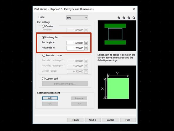
Now you need to specify the dimensions of the pads. The pads are the conductive areas on your PCB where the leads (legs) of your components will make contact with the board and have traces (wires) connect to it.
-
The pad dimensions can be inferred from the datasheet by looking at the dimensions of the leads. Create pads that are slightly larger (roughly 5% to 10% in all directions, if there is clearance) than the leads of your component.
-
Again, datasheets will often provide you with pad dimensions and spacing. In this particular case the information is not provided so we are forced to determine our own pad size.
-
Don’t worry about pin count or spacing yet. These issues will be addressed in the next step.
-
Click Next when you are done.
-
-
-
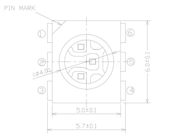
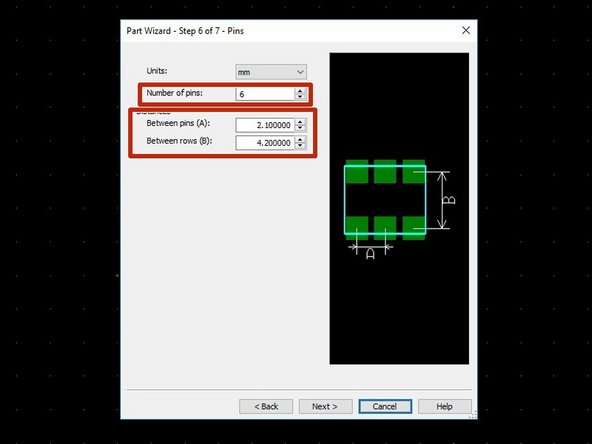
Now specify the pin count, pin pitch (distance between adjacent pin centers - measurement A in Ultiboard) and the distance between centers of each pin row (measurement B in Ultiboard).
-
The between-row value of 4.2mm shown in the example here was determined as follows:
-
Datasheet specifies the distance from pin edge to pin edge as 5.7mm. We added 0.1mm to each dimension of the pads previously, so the total distance from pad edge to pad edge is 5.7 + 2(0.1) = 5.9mm.
-
To measure the distance from center to center of the two rows, subtract half a pad width from either direction: 5.9 - 2*(½)*1.7 = 4.2mm.
-
Click Next when you are done.
-
-
-
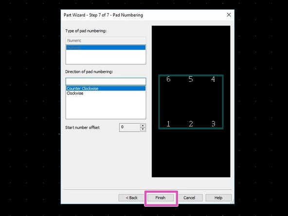
In the final window, confirm that the pin numbering is correct (refer to the datasheet) and make any adjustments necessary for your component.
-
When you are done, click Finish.
-
-
-
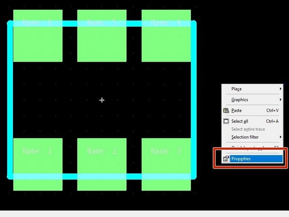
You will now see your completed footprint on the screen.
-
You should add a reference designator so that the part is easily identifiable. Right click the footprint and choose Properties.
-
-
-
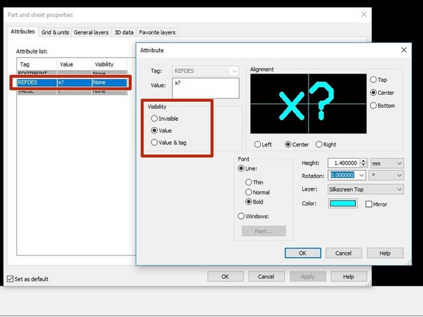
In the Attributes tab of the window that appears, be sure to change the REFDES visibility from Invisible to Value.
-
Click OK in both windows when you are done.
-
-
-
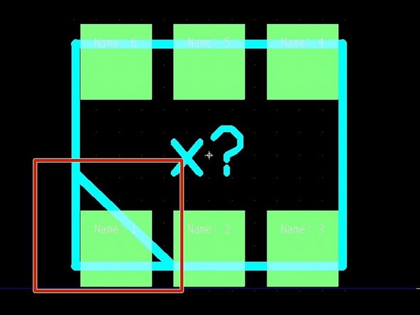
Notice that the footprint is symmetric. In order to ensure the component is oriented properly when placed, it is necessary to add the corner cutoff mentioned previously. Perform this manually by placing a line.
-
Use the Ultiboard menus: Place -> Graphics -> Line.
-
Be sure to put the notch at the corner where pin 1 is located. Note that you can view pin numbers temporarily by zooming in on the footprint.
-
-
-
The footprint is now complete. Save the footprint to your Ultiboard user database.
-
Give the footprint the same name as the component, CLP6C-FKB-CK1P1G1BB7R3R3.
-
-
-
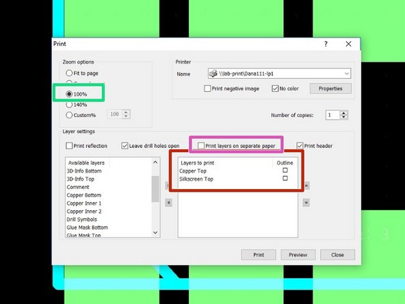
As a final check, you should always print out your newly created footprint on a one to one scale (100% zoom).
-
Choose File -> Print from the toolbar. Apply the following settings in the Print dialogue before printing your footprint:
-
Move the layers Copper Top and Silkscreen Top from the Available layers box to the Layers to print box.
-
Configure zoom to 100%.
-
Uncheck Print layers on separate paper.
-
-
-
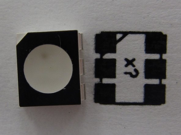
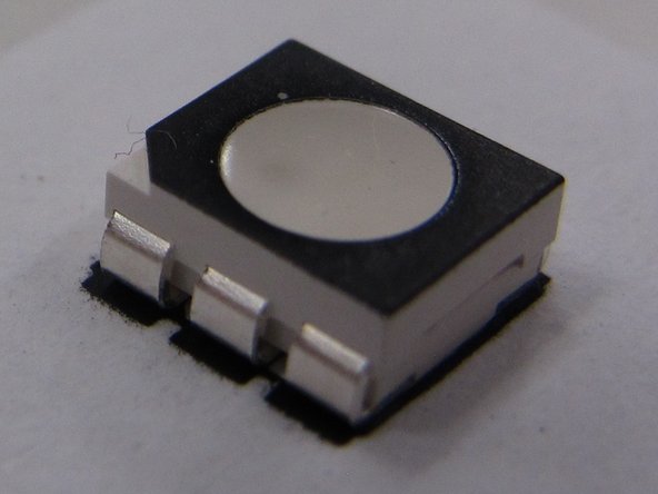
Always place the physical component on top of the newly created footprint on paper. Make sure that all leads, pins, slots, etc. line up exactly with your footprint. If anything needs to be corrected, go back into Ultiboard, make the modifications necessary, and re-print your footprint. Check again and save as necessary.
-
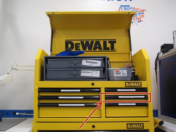
Firefly components are available in the Maker-E. Check the yellow DeWalt cabinet for the labelled "Firefly" drawer.
-
-
-
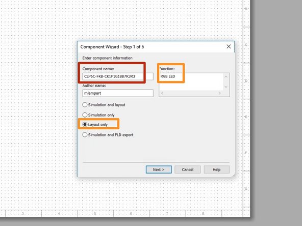
With the footprint created in Ultiboard, you are now ready to return to Multisim. Launch the Component wizard (Tools -> Component wizard) and enter the manufacturer part number for the component name.
-
Provide a brief description of the component, and choose to create a Layout only.
-
-
-
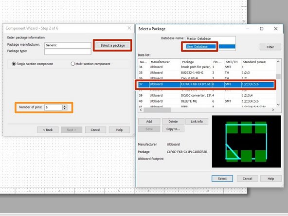
In the next window you will be prompted to choose a package. Click on the Select a Package button and navigate to your user database. Locate the footprint you created previously.
-
Be sure to update the Number of pins field after choosing your footprint.
-
Click Next when you are done.
-
-
-
The next window instructs you to create a schematic symbol for the component. This is how the component will be represented in Multisim (as opposed to the footprint, which is how parts are represented in Ultiboard).
-
Whenever possible, copy the symbol from an existing part in the master or corporate databases. While it is possible to create your own symbols, the symbol editor is cumbersome.
-
For this tutorial, please copy the existing symbol from the component in the Corporate database.
-
Once you see the symbol displayed correctly click Next to continue.
-
-
-
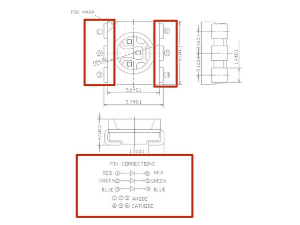
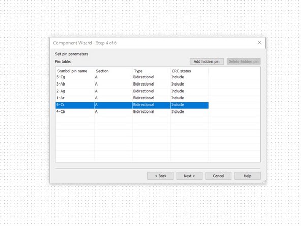
Step 4 of the wizard allows you to assign descriptive names to each of the pins of your symbol.
-
Refer to page 7 of the datasheet for the proper pin names/descriptions.
-
You have the option of displaying or hiding symbol pin names in your schematic. For multipin devices, such as ICs, this is helpful for determining the function of the otherwise identical pins. Hence, it is always a good idea to label the pins of your schematic symbol.
-
Try to keep pin names short. This will result in smaller, more manageable schematic symbols.
-
Click Next when you are done.
-
Prior to 3/06/2018 this step had an inaccurate image for the pin mapping. The current version you are reading now has the accurate image.
-
Prior to 3/15/2018 the Multisim schematic symbol for the CLP6C-FKB-CK1P1G1BB7R3R3 component in the Corporate database had improperly labelled pins. This issue has since been resolved. If you created your CLP6C-FKB-CK1P1G1BB7R3R3 part prior to this date it will need to be corrected.
-
-
-
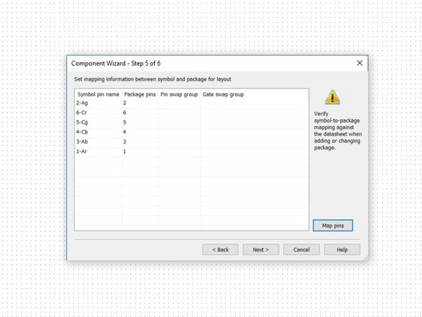
Now you need to map the symbol pins to the footprint pins. Typically the mapping is one to one.
-
Click Next when you are done.
-
-
-
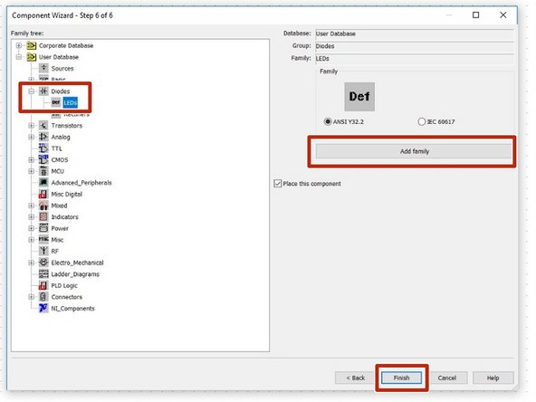
Your component is now complete. Save the component to your Multisim user database. You may need to add a family as a subcategory under one of the pre-defined categories before Multisim will allow you to save the component.
-
In this example we have created a family called LEDs as a subcategory under the provided Diodes category.
-
Click Finish when you are done.
-
Note that when you save the Multisim component, it is now linked to the Ultiboard footprint you created previously.
-
-
-
Now place your newly created RGB LED and connect it in series with the IR LED (QEE113) and the resistor(s) you chose previously.
-
-
-
Congratulations! You are now done designing your firefly circuit in Multisim.
-
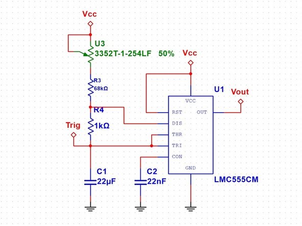
Confirm that you added all of the components and made all of the proper connections by comparing your final circuit to the completed circuit in the example here.
-
For a hi resolution version of the full circuit, please follow this link.
-
Note that all of the circuit elements appear here in either blue or green. If any of your circuit elements appear in black this means that they do not have a footprint associated with them.
-
If you were to transfer your circuit to Ultiboard for PCB layout, any components which are shown in black in Multisim would not appear in Ultiboard because they have no physical representation associated with them.
-
If your circuit has components displayed in black you will need to add footprint information to these components prior to transferring your circuit to Ultiboard.
-
-
-
You are now ready to move on to Ultiboard to lay out the physical connections of your printed circuit board.
-
You can find the Ultiboard tutorial here.
-


Cancel: I did not complete this guide.
22 other people completed this guide.