
Introduction
If you create a part for a personal project and think that it may benefit other makers, send it to us!
For more information, please see NI's guide for creating boards.
-
-
For the purpose of this guide, we will be creating a footprint for a CLP6C-FKB-CK1P1G1BB7R3R3.
-
We will begin by creating a custom footprint for the LED. Because footprints correspond to the physical realization of electronic components, you will need to use Ultiboard. Launch Ultiboard and followthis tutorial on the right to familiarize yourself with the process of creating a custom footprint.
-
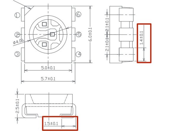
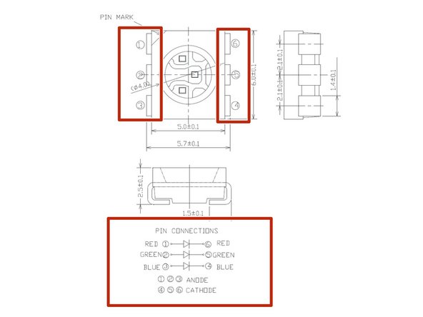
The datasheet for this part is in the details section. Open the datasheet and examine page 7. Often datasheets will give you a defined footprint with dimensions of pads, pin pitch, etc. This datasheet does not go that far so it is up to you to infer footprint pad size, pitch, and other parameters from the measurements of the component itself.
-
You may skip the "3D Land Pattern" portion of the NI tutorial.
-
-
-
Before creating the component, you should become familiar with the datasheet. The important features of the datasheet to look for (for PCB production):
-
Land Pattern ( Also called "recommended PCB pattern")
-
Pin mappings
-
A link to the datasheet for the LED can be found here. Open the datasheet and examine page 7, highlighted here. Often datasheets will provide a defined footprint with dimensions of pads, pin pitch, etc. This datasheet does not go that far so it is up to you to infer these parameters from the measurements of the component itself.
-
-
-
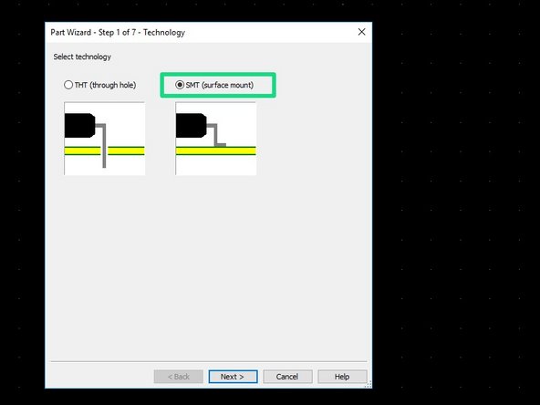
With Ultiboard open, choose to create a new project of type PCB design. Launch the Part wizard in Ultiboard (Tools -> Part wizard) and choose to create a surface mount (SMT) part.
-
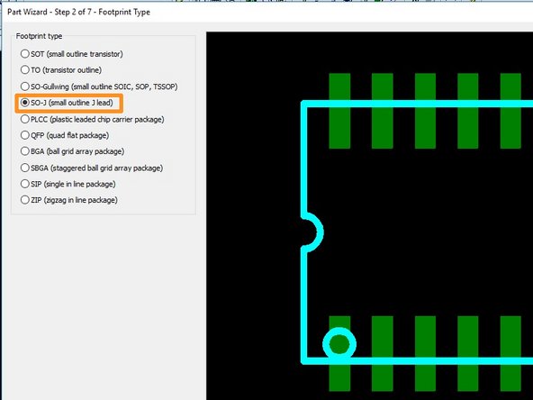
Our LED is in a package type called SOJ (small outline J-lead). Choose the appropriate footprint type in the next window. Don’t worry about the fact that the number and location of pins do not match our LED. We will correct this shortly.
-
If you would like to see more information about package sizes, please see the PCB in the lab bench underneath the pick and place.
-
-
-
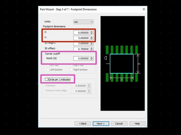
Set your dimensional units to match what is given on your datasheet. In this case the measurements are metric, so choose mm.
-
You need to specify the dimensions of the entire plastic component package. Examine the datasheet for this information. Note that there are tolerances (±) associated with many of the dimensions. For now we will ignore these
-
Our LED has a corner cutoff in the top left corner, near pin 1. We will add this later. For now, set the Notch value to 0 and uncheck the Circle pin 1 indicator.
-
What you have done is create an outline of the space on your PCB that will be occupied by your component.
-
The next screen (3D color settings) is not relevant, and can be ignored. You can proceed to step 5
-
-
-
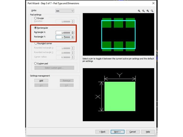
Specify the dimensions of the pads. Pads are conductive areas on your PCB where the leads (legs) of your components will make contact with the board and have traces (wires) connect to it. The pad dimensions can be inferred from the datasheet by looking at the dimensions of the leads.
-
The pad dimensions can be inferred from the datasheet by looking at the dimensions of the leads. Create pads that are slightly larger (roughly 5% to 10% in all directions, if there is clearance) than the leads of your component.
-
Datasheets will often provide you with pad dimensions and spacing. In this particular case the information is not provided so we are forced to determine our own pad size.
-
Continue to step 6 to select pin sizes.
-
-
-
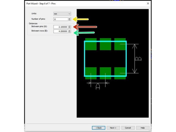
Now specify the pin count
-
Now specify the pin pitch (distance between adjacent pin centers - measurement A in Ultiboard)
-
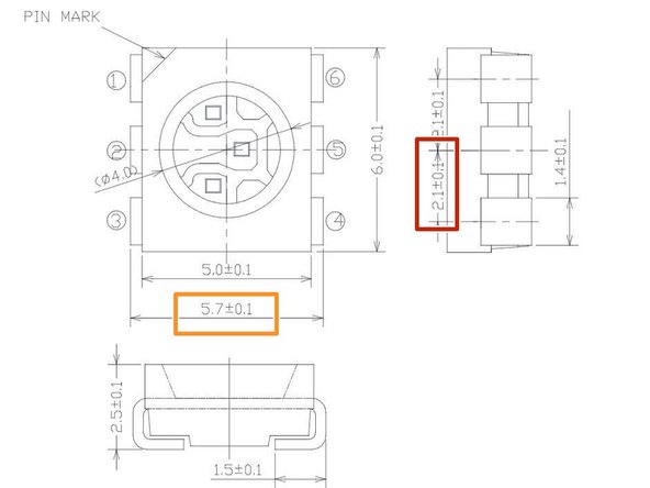
Specify the distance between centers of each pin row (measurement B in Ultiboard). The between-row value of 4.2mm shown in the screenshot at right was determined as follows:
-
Datasheet specifies the distance from pin edge to pin edge as 5.7mm. We added 0.1mm to each dimension of the pads previously, so the total distance from pad edge to pad edge is 5.7 + 2(0.1) = 5.9mm.
-
To measure the distance from center to center of the two rows, subtract half a pad width from either direction: 5.9 - 2*(½)*1.7 = 4.2mm.
-
-
-
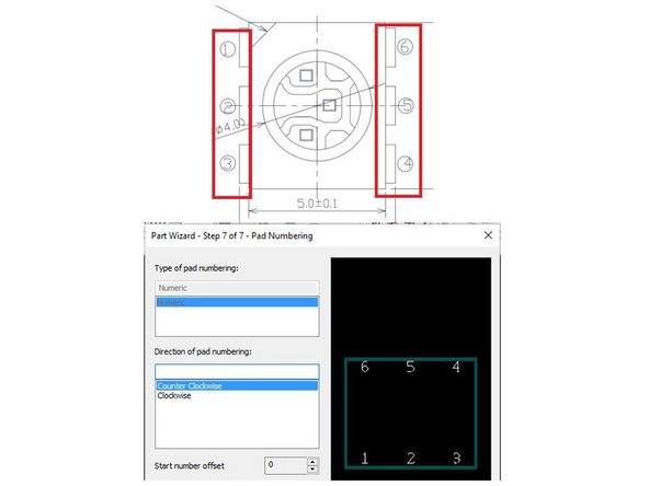
In the final window, confirm that the pin numbering is correct and make any adjustments necessary for your component.
-
When you are done, click Finish.
-
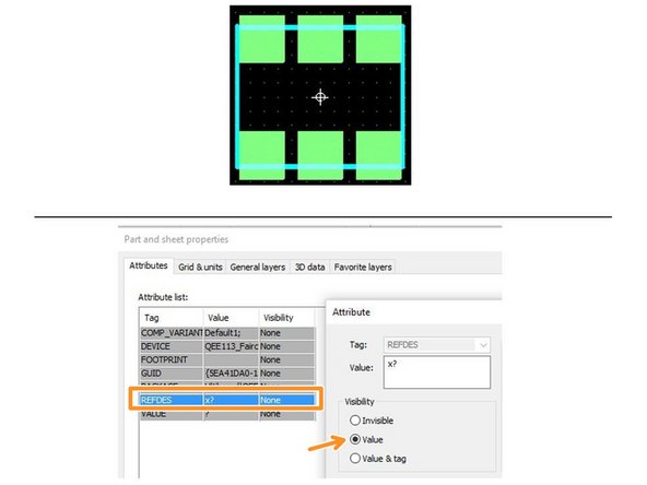
You will now see your completed footprint on the screen. You should add a reference designator so that the part is easily identifiable. Right click the footprint and choose Properties.
-
In the Attributes tab of the window that appears, be sure to change the REFDES visibility from Invisible to Value.
-
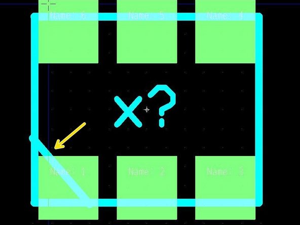
Notice that the footprint is symmetric. In order to ensure the component is oriented properly when placed, it is necessary to add the corner cutoff mentioned previously. Perform this manually by placing a line: Place -> Graphics -> Line.
-
Be sure to put the notch at the corner where pin 1 is located. Note that you can view pin numbers temporarily by zooming in on the footprint.
-
-
-
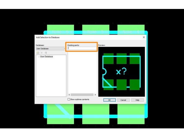
The footprint is now complete. Save the footprint to your Ultiboard user database. Select File -> Save to Database
-
Give your part a name. We suggest using the manufacturer part number as opposed to something generic like "LED"
-
If your user database is not showing up, please see Adding Databases to Multisim, and if you have not created a user database yet, please see this guide. If you don't know what this means, follow the guide to do so, and heed the below warning.
-
If you have not specifically created a user database, the user database that is showing up is WRONG! If you do not create a new database according to the tutorial in the previous step, your part may be automatically deleted when windows restarts. If in doubt, check!
-
You will need to re-add your user database EACH time you open Multisim on a new computer. It is a hassle but doing so will prevent later headaches.
-
-
-
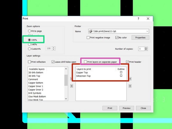
As a final check, you should always print out your newly created footprint on a one to one scale (100% zoom).
-
Choose File -> Print from the toolbar. Apply the following settings in the Print dialogue before printing your footprint:
-
Move the layers Copper Top and Silkscreen Top from the Available layers box to the Layers to print box.
-
Configure zoom to 100%.
-
Uncheck Print layers on separate paper.
-
-
-
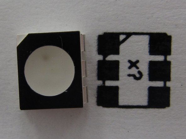
Always place the physical component on top of the newly created footprint on paper. Make sure that all leads, pins, slots, etc. line up exactly with your footprint. If anything needs to be corrected, go back into Ultiboard, make the modifications necessary, and re-print your footprint. Check again and save as necessary.
-
Firefly components are available in the Maker-E. Check the yellow DeWalt cabinet for the labelled "Firefly" drawer.
-
-
-
With the footprint created in Ultiboard, you are now ready to return to Multisim. Launch the Component wizard (Tools -> Component wizard) and enter the manufacturer part number for the component name.
-
Provide a brief description of the component, and choose to create a Layout only.
-
-
-
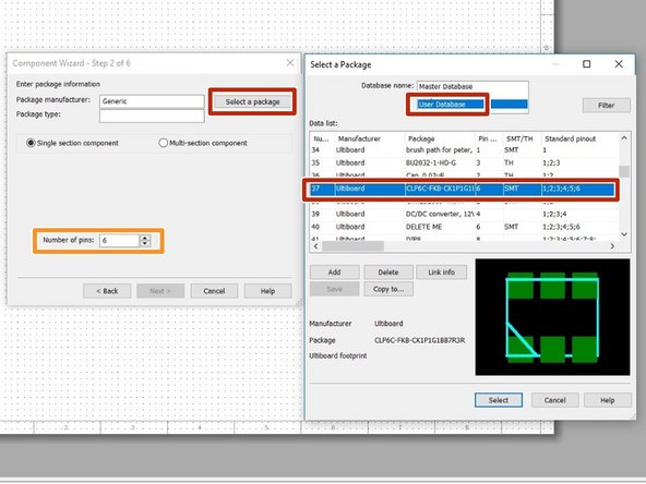
In the next window you will be prompted to choose a package. Click on the Select a Package button and navigate to your user database. Locate the footprint you created previously.
-
Be sure to update the Number of pins field after choosing your footprint.
-
Click Next when you are done.
-
-
-
The next window instructs you to create a schematic symbol for the component. This is how the component will be represented in Multisim (as opposed to the footprint, which is how parts are represented in Ultiboard).
-
Whenever possible, copy the symbol from an existing part in the master or corporate databases. While it is possible to create your own symbols, the symbol editor is cumbersome.
-
For this tutorial, please copy the existing symbol from the component in the Corporate database.
-
If you need information about databases, please see this page.
-
Once you see the symbol displayed correctly click Next to continue.
-
-
-
Step 4 of the wizard allows you to assign descriptive names to each of the pins of your symbol.
-
Refer to page 7 of the datasheet for the proper pin names/descriptions.
-
You have the option of displaying or hiding symbol pin names in your schematic. For multipin devices, such as ICs, this is helpful for determining the function of the otherwise identical pins. Hence, it is always a good idea to label the pins of your schematic symbol.
-
Try to keep pin names short. This will result in smaller, more manageable schematic symbols.
-
Click Next when you are done.
-
-
-
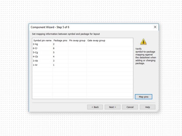
Now you need to map the symbol pins to the footprint pins. Typically the mapping is one to one.
-
Click Next when you are done.
-
-
-
Your component is now complete. Save the component to your Multisim user database. You may need to add a family as a subcategory under one of the pre-defined categories before Multisim will allow you to save the component.
-
In this example we have created a family called LEDs as a subcategory under the provided Diodes category.
-
Click Finish when you are done.
-
Note that when you save the Multisim component, it is now linked to the Ultiboard footprint you created previously.
-
Congratulations! You have now created your own custom component. If you think that this is a component that would be useful for other makers, please send it to us!
-
The process for creating this component was not specific to this part. Other parts will be different and will have different parameter, pin maps, packages, etc but the general process is the same.
-


Cancel: I did not complete this guide.
One other person completed this guide.