
Introduction
The Maker-E offers the ability to design and simulate circuits in software, as well as lay out a physical printed circuit board (PCB). The Maker-E supports two software packages for this purpose: NI Multisim/Ultiboard and Altium Designer. This tutorial will focus on Multisim and Ultiboard, as these are designed to be easy to use, with a relatively full feature set. If you wish to explore Altium Designer, please contact the Lab Director.
Published by Matt P. Lamparter with contributions from Daniel T. Vasquez.
-
-
A circuit can be designed in software to allow the connection of various electronic components, power sources, and measurement devices. Each element is represented by a schematic symbol.
-
-
-
Simulating a circuit can provide you with an idea of how it will behave under certain conditions without having to physically construct and test the circuit. This can save the designer considerable time and money.
-
Note that a simulation is only as good as the mathematical models upon which it is based.
-
These tutorials will not cover the circuit simulation feature of Multisim.
-
-
-
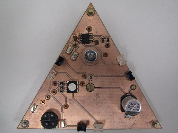
A PCB is the physical realization of a circuit. After designing and simulating a circuit in software, you are ready to physically connect all of the components together on a single board.
-
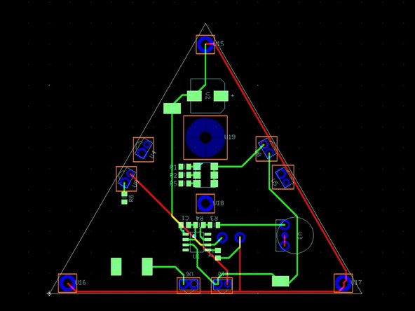
Using PCB design software, you can place component packages (physical realizations of circuit elements) and connect them with traces (wires on the PCB).
-
When your PCB design is complete you can fabricate the board in the Maker-E, or send the board to an external company for professional manufacturing.
-
-
-
The benefit to creating a PCB in the Maker-E is that it is significantly faster than sending files to a company and waiting potentially several weeks for your board(s) to return.
-
PCBs fabricated in the Maker-E do have some limits, but for most rapid prototyping the PCBs created in the Maker-E are adequate.
-
To begin learning the software we use to design PCBs at the Maker-E, complete this guide below and follow the link here
-


Cancel: I did not complete this guide.
8 other people completed this guide.